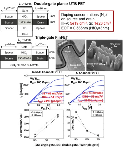
Tri-Gate FinFETs
As device shrinks, novel concept devices and/or better materials than Si are required. The integration of III-V is mainly driven by the high electron mobility of these materials. Also, Tri-gate structure is the most favourable architecture for Lg scaling due to SCE degradation. We combined all these benefits to compare the properties of III-V (InGaAs) and Si MOSFET / FinFETs at short gate length. Here we demonstrate where this technology is a viable alternative to Si in the next successive node of the ITRS.
|
Objective:
Approach:
Results/Impact:
|
|
Group member involved:
- Seung Hyun Park
- Mehdi Salmani
- Gerhard Klimeck
- Mark Lundstrom
- Mathieu Luisier