Objective:
- Contact resistance is becoming a critical factor in device on-state performance.
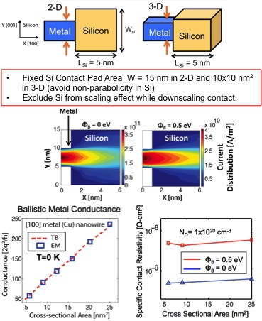
- Investigate scaling effect on specific contact resistivity in Metal-Si contact structure.
Approach:
- Quantum transport simulation for 2-D / 3-D Metal-Si structure.
- EM model calibrated against TB model: Fit ballistic conductance of metal (Cu) wire in EM with TB .
- Include Shottky barrier(ΦB) between M-Si and vary doping concentration in Si contact pad region (>1e20 cm-3)
Impact:
- Lower Schottky barrier and high doping concentration drives lower resistivity.
- Metal conductance linearly decreases as while downscaling.
- Contact resistivity is almost constant while downscaling cross sectional area of metal interconnect.
- Surface roughness and grain boundary are expected to cause the conductivity degradation in metal wire.
- Present in DRC and IWCE (2013).
|
 |

