Contact resistance modeling of HEMT device
The contact-to-channel series resistance is becoming more important issue as the channel length is scaled down. We are exploring the physical origin of the contact resistance through quantum simulations and finding better structure in the engineering point of view.
Realistic Contact-to-Channel Modeling and Analysis InGaAs/InAs HEMT
Objective:
- Guide III-V HEMT design to obtain better performance by exploring realistic contact-to-channel resistance model
Approach:
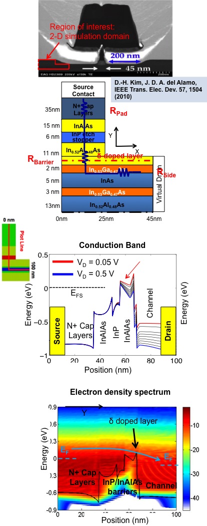
- Large-scale atomistic transport simulation -> real-space EM simulation.
- NEGF and Poisson for 2-D geometries.
- Non-parabolicity from TB fitting.
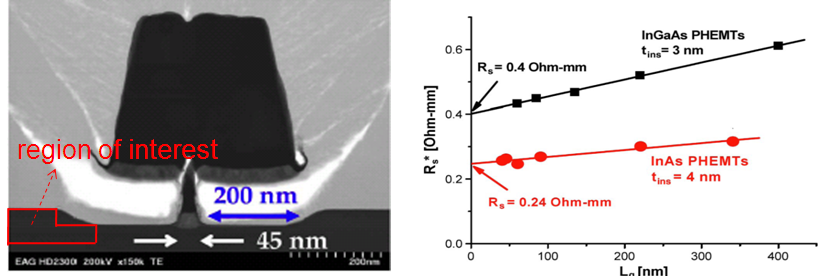
- Resistance factors: barrier layer, curved area, and phonon scattering.
- Analyze band diagram, electron density, and resistive characteristics.
Impact/Preliminary Results:
- Detail understanding of transport property in contact-to-channel region in hetero-structures.
- Thick InAlAs barrier plays the main role in the series resistance.
- Best Poster Award in IEEE NMDC.
- Prepare for a publication.
Simulation Results:
- Electrons are well-thermalized due to phonon interaction.
- Non-parabolicity is included. -> Bulk EM model over-predicts Fermi level.
- Extracted contact resistance at very low drain bias (10mV) .
- Low field phonon mobility extraction .
- Thick InAlAs barrier is the main factor in contact-to-channel resistance.
|
 |
Group member involved: