Emerging scanning tunneling microscope (STM) lithography and low-temperature molecular beam epitaxy (MBE) has opened up the possibility of controlling donor positions within a few atomic mono-layers. Based on this technology, experimentalists have suggested various prototypes of planar patterned densely phosphorous δ-doped Si (Si:P) devices with the motivation stemming from potential utilities in quantum computing applications as well as possible solutions for ultimate device scaling. We investigate the electronic properties of Si:P electron reservoir and ultra-thin wire of atomic scale are investigated using NEMO 3D that will provide valuable understanding to contacts and leads in single impurity devices.
Electronic properties of the disordered Si:P δ-doped layer
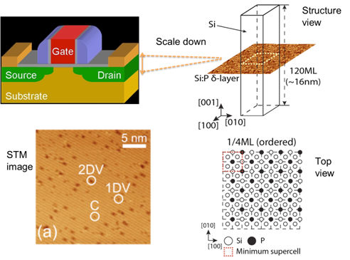
Si:P δ-doped layer serves as a contact region in variety of Si:P devices. Experimentalists can now fabricate a perfect 2D system with negligible vertical straggle. As a result, this technology can be used for solid-state quantum computing applications and shallow contacts for ultra-scaled MOSFET devices.
In this study, we are pursuing answers on following items:
Validation of our atomistic self-consistent methodology for bandstructure calculation using NEMO 3D
Investigation of atomistic effects, such as dopant disorder in the δ-layer
(Ongoing) Comparison between theoretical results and spectroscopy data to determine the valley position in the impurity bands
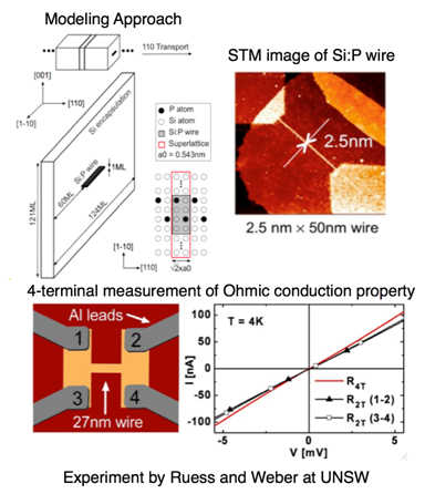
Si:P Nanowires (1-D)
The structure of Si:P nanowire is depicted in the figure below. Phosphorous donors are placed in a narrow doping region by bulk silicon. The wires can potentially be the next-generation interconnects for further downscaled devices.
There has been extensive experimental effort in studying and fabricating Si:P devices. Our theoretical study is aimed at aiding experimental study and guiding potential device designs. Experimentalists have raised several key questions which are the main focus of our study.
(1) Can we confirm that the system has a metallic?
(2) What is the spatial extent of the channels?
(3) Can the channels be modulated and in what limits?
(4) What is the role of impurity placement fluctuations?
Group Members Involved:
Network for Computational Nanotechnology, Purdue University