The schematic was significantly updated and can be seen in Yuri's notebook in the near future. Most of the data lines between the various modules are known and connected.
January 8, 2008(2 hours):
We met as a team after class to discuss preliminary project proposal.
January 9, 2008(1 hour):
We worked with the website to get the lab notebook feature to work. We also disucessed meeting with a patent lawyer.
WEEK 01 SUMMARY
Accomplishments: Submitted preliminary project proposal.
Weekly Work Total: 3 hours
Project Work Total: 3 hours
January 14, 2008 (2 hours):
We met as a team to formulate PSSC for presentation in class on 1/16/08.
January 15, 2008(5 hour):
Researched design constraints, components, and packaging.
Also, researched OBEX for OS handshaking.
Met as a team to discuss tommorow's presenation about PSSCs (Project Specific
Success Criteria). Started work on Homework 2 and finished the abstract and project description. The block diagram and deciding how to break up the workload still needs to be done.
January 17, 2008 (3 hours):
We met as a team to finish the final project proposal.
January 19, 2008 (1 hours):
I researched how existing USB flash drives work.
WEEK 02 SUMMARY
Accomplishments: Submitted preliminary project proposal.
Weekly Work Total: 6 hours
Project Work Total: 9 hours
January 21, 2008 (3 hours):
I did further research on Bluetooth modules, NAND Flash, and Flash memory controllers.
January 22, 2008 (4 hours):
Morning: I continued the component research and found the following Bluetooth modules:
Bluetooth 2.0 and EDR Class 2 Module with UART Support
Model Number:QBTM500
www.zbausa.com/pdf/Module%20BT44-191C.pdf
Some key features include a built-in ptinted PCB antenna, USB 2.0 compatible, UART support, and different power modes.
Some cons include lack of documentation and it is newly developed.
Also, found bluetooth modules available at:
Broadcom Bluetooth Modules
* Cons all single chip solutions are WLBGA or FPGA package scales
QCOM Bluetooth Modules
Evening: We met togther as a team to discuss the component contstraints and began to finalize them. Did some team brainstorming and discussion on modular design.
Also disucssed the file system we plan to use. Fat32 is what we chose based on its ability to handle larger files (media) and its ability to work with all of
the modern OS's.
January 23, 2008 (2 hours):
I researched power constraints and how the battery and appropriate charging circuit would function.
Lithium-ion was chosen as are battery type based on weight and size constraints.
However, the charging circuit has to be able to handle Lithium-ion's under and over voltage requirements.
WEEK 03 SUMMARY
Accomplishments: Narrowed down major component choices and design constraints
Weekly Work Total: 9 hours
Project Work Total: 18 hours
January 28, 2008 (7 hours):
Morning:
We met as a team with a EET professor about how to implement different surface-mount packages including QFN, DFN, and BGA.
He is ging to allow us to use the reflow oven in the EET lab and even offered to guide us through the process.
This means QFN and BGA packages can still be used if we need them in our design.
Also, met as a team to discuss the design constraints and try to finalize our microcontroller choice.
Evening: Met as a team to finalize our design constraints and narrow our part selection.
The following list shows our constraints so far for each component (are subject to change):
Microcontroller:
Periperals needed include TIM for controlling pusbutton and LED blinking, ATD for looking at battery voltgate, and SPI for communications to Bluetooth module.
Also, around 20 pins of General IO are desired, but is extermely open to change as needed. Also, power consumption is a concern.
Processor speed is not an issue because the Bluetooth and Flash Controller Modules will be handling the data transfers.
Memory:
We are using NAND Flash for its improved duribilty over other memory types.
256MB to 1 GB is desired. It should be enough to store several types of files on and possibly some media.
Power consumption is a concern as well as writing and reading speeds.
Flash Memory Controller:
Needs to interface easily with USB protocol
Need to discuss 8 bit vs. 16 bit bus width
Charging Circuit:
Speed of charging the battery. It needs to be "user friendly fast".
Needs to charge a 3.7V Lithium-Ion battery.
Needs to have the over/under voltage charcteristcs needed by the Li-ion battery.
Battery:
Needs to be small enough for use in a portable device
Needs to be able to power the device for several hours and recharge quickly
January 29, 2008 (7 hours):
Morning: I worked with Yuri to come up with final microcontroller and Bluetooth module ideas to pitch to group.
Decided on using PIC18F2455 microcontroller instead of the Atmel with USB. Also, emailed Roving Networks about using their device for Bluetooth file transfer.
They said that their device acts like a Serial port and does not utilize OBEX like we desired. Exchanged emails with the EET RF professor about PCB board design.
The WT12 Bluetooth module's datasheet suggests that we put a ground plane above and below above all data lines to and from the module. This may create the need for a 4-layer PCB.
Evening: We met as a team to discuss the Design Constraint Analysis Report due Friday and the TCSP presentation.
Finalized the TCSP powerpoint that Scott will present. Also, found another company to provide our Bluetooth module (Ezurio).
I am in communication with a sales representive from the company to further discuss the BISM II module, specifically its claims in being able to do FTP with Windows OS.
January 30, 2008 (5 hours):
Morning: I met with Yuri to pick up the Tablet PC. Also, exchanged emails with the Ezurio sales representive.
The module can send and recieve files using FTP according to the datasheet as well as the sales rep. This module is also well documented, but is slightly larger than the WT12, which is the other canidate.
Evening: We met as a group to finalize components for the Design Constraint Analysis Report. Found that the Bism II w/ USB
may be the best choice for the Ezurio Bism II Bluetooth Module family based on the fact it does USB stacking inside of the Bluetooth stack.
I also went through the data sheets of the chosen parts and computed the typical and maximum power usage so we can succesfully choose our battery to fit our needs.
For typical use we desire 10 hours of data transfer. This means we need a battery of at least 1200 mAh. Based on research of batteries we found a 1700 maH battery from Ultralife and the link can be found in Yuri's notebook.
Bluetooth Module 30 mA @typical and 50mA @max
Microcontroller 1.3 mA @typical and 3mA @max
Flash Controller 25 mA @typical and 35mA @max
NAND Flash 10 mA @typical and 20mA @max
Total Power Usage 66.3 mA @typical and 108mA @max
DC to DC converter efficiency 90%
Actual Power need from battery to operate components ~75mA @typical ~120mA @max
January 31, 2008 (1 hour):
I recieved an email from the Ezurio about the TRBLU024-00100 - Embedded USB / HCI Bluetooth?Module, which I thought may be an easy implentation
for us to comunicate from the Bluetooth Module to the Flash controller. However, this module requires we run a embedded OS and third party software
on a microcontroller, neither of which they are willing to support. Thus, we will not use the Embedded USB / HCI Bluetooth?Module, but the BISM II Module
made by the same company. They are not willing to give us samples, so the cost of development has increased as expected. The cost is similar to the other Bluetooth Modules
with the module costing $67 and the evaluation board costing $180. The part and respective evaluation board can be found at Mouser by clicking the links below.
TRLU23-00200 - BISM II Module
BISDK02BI-02 - BISM II Development Kit
WEEK 04 SUMMARY
Accomplishments: Design Constraint Analysis TCSP Presentation and Report and Finalized Major Component Selection
Weekly Work Total: 20 hours
Project Work Total: 38 hours
February 4, 2008 (3 hours):
We met as a team to discuss the packaging requirements and footprint.
Products that are packaged similar to ours include a flash drive and portable hardrive. The Ezurio Bluetooth module and evaluation board were ordered
from Mouser.com. See the links above for more information. We decided that we cannot use the NAND Flash Memory Controller and Memory from ST that we
choose earlier because we cannot find any distrubutors. Also, the sales staff as faied to answer any of our questions.
We are continuing the search for the memory controller and memory, and hope to have the parts ordered by tommorow.
February 5, 2008 (6 hours):
Morning: I tried to contact STMicroelectronics about sampling a Flash Controller and NAND Flash from them. I called both the Kokomo and Indianapolis sales offices,
but neither offices picked up the phone during various calls throughout the day. Continuing the search for the Flash controller and memory I contacted
USBest, but decided not to order from them because of part availability.
Evening: Looked at all the datasheets ordered and collected physical size requirments from each part. It can be seen in this spreadsheet.
Important criteria that arose from this analysis include thickness and weight. The battery is most of the weight at 41 grams. This makes our device too heavey to function
as a typical flash drive, where it hangs from the USB port. Therefore, either a USB cable will have to be supplied or even a retractable cable could be used.
The Bluetooth Module is adding several millimeters of thickness and has to be mounted above the "mother" PCB board (the board we are designing.)I thought a package similar to a portable
1.5" or 2.5" harddrive would prove to be effective for our design. it would be durable and light weight. Also, heat may be a concern from our charging circuit so venting may be required in our packaging design.
I found a NAND Flash Memory IC from Micron and request samples. It matches our Flash controller already ordered.
February 6, 2008 (2 hours): We went into the lab to ask about FLASH memory controllers and Flash Memory, but no TA's were available.
I have recieved no word from the Micron sales office about a sample, and proceeded to search for in-stock Flash memeory. I contacted the Ezuiro sales rep about the surface mount package for the
Bluetooth module. He replied saying the surface mount option requires a firmware upgrade that involves an RS232 header and respective hardware. He gave us several ideas for mounting the bigger module thought.
The one that is the best solution for our design is to mount the module on the HIROSE header and some other hardware. We can populate the underneath the Bluetooth module as long as the antenna is not within 2mm in any direction of any of our parts.
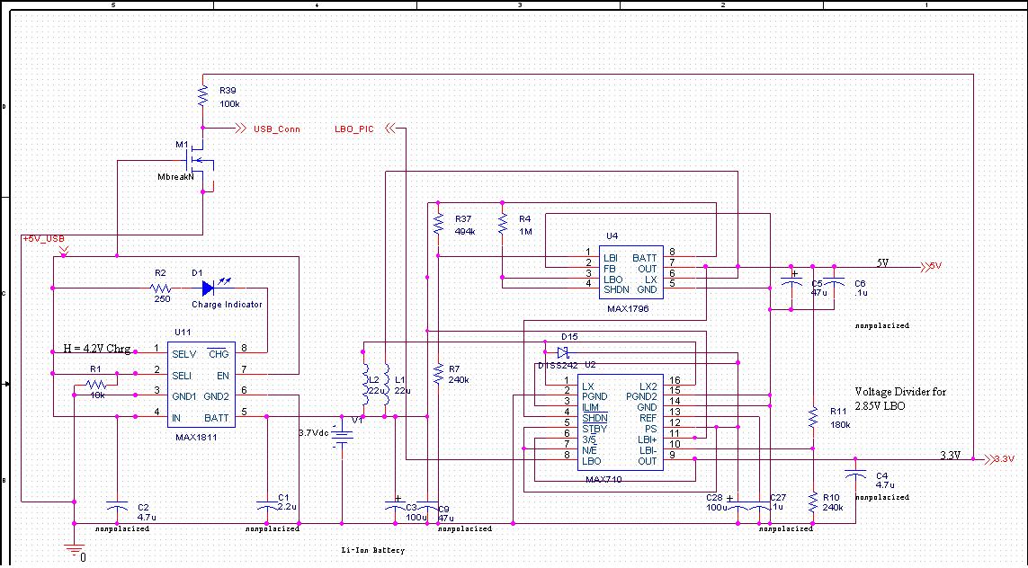
I also looked over Yuri's power supply and recharging circuit and had him explain how it worked and how the values
for the passive parts were chosen. The circuits seems feasible and an effective solution.
February 7, 2008 (2 hours):I met with Yuri to discuss further part selection including some passive elements. The datasheet
for the DC-to-DC converter specifices certain passive elements, and we decided that those should be strictly adhered to.
A parts list was created and an order is plan to placed this evening. We also looked at other vendors for our battery since Mouser said it was
going to take six weeks for shipment. No other vendors were found and other Li-ion batteries were discussed but none were ordered as of yet.
WEEK 05 SUMMARY
Accomplishments: Packaging constraints, footprints of all major components, power supply circuit including recharging circuit,
Weekly Work Total: 13 hours
Project Work Total: 51 hours
February 11, 2008 (1 hour): I met with Yuri and Scott to catch up on the progress of the project. All major components beside the NAND Flash
IC have been shipped. The Bluetooth module is in hand and text can be sent between computers using a Bluetooth Dongle and the Ezurio Bluetooth Module. I emailed the
Ezurio sales representative about FTP transer from the Bluetooth moudle. The previous documention that was provided was corrupt and crashed the .pdf reader.
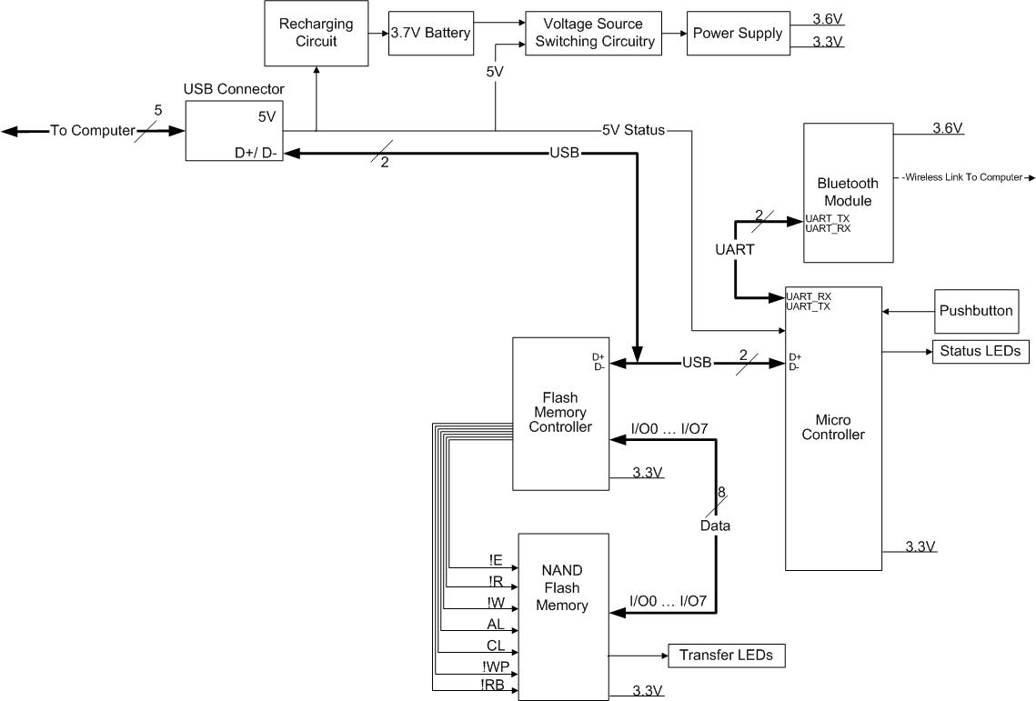
February 12, 2008 (6 hours): We met as a team to disuss the harware description of our device. Several important flaws in our design were found. This led to an involved discussion of
our design and the role the microcontroller will play. We decided that the micro controller will have to be sent data from the Bluetooth Module via UART and
change that to USB. This will really increase the difficulty of the software that is going to have to be written, but we found that our Bluetooth Module does
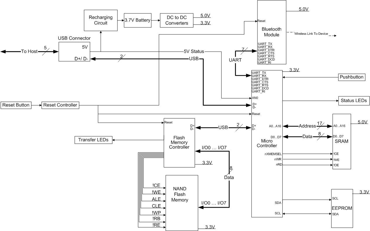
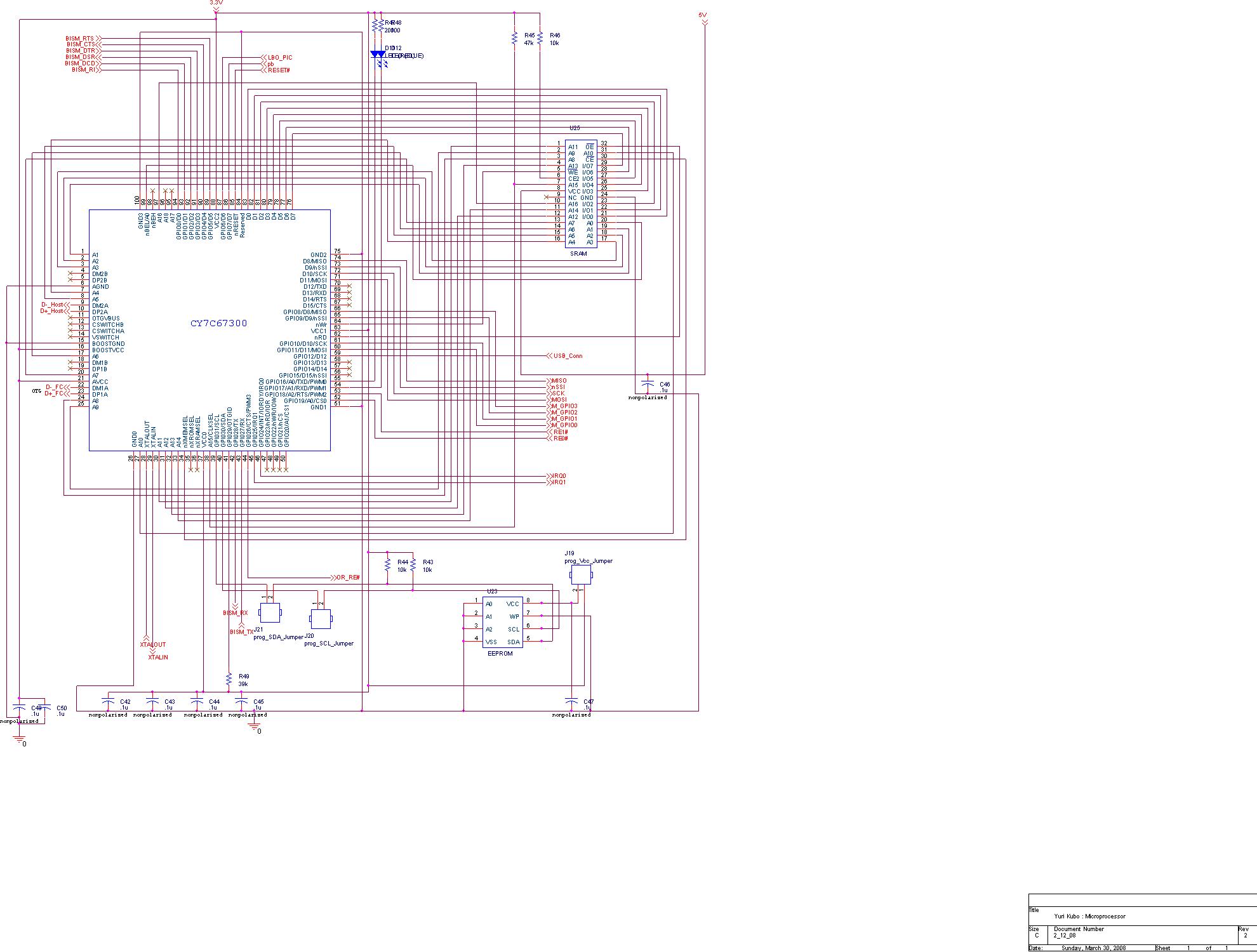
not send data over the USB lines, but a firmware upgrade may be available. I updated the Block Diagram accordingly and it can be seen below:
The schematic was significantly updated and can be seen in Yuri's notebook in the near future.
Most of the data lines between the various modules are known and connected.
February 13, 2008 (5 hour): I received the firmware upgrade for the BISMII module and forwarded it to Scott, so he could implement it on the module.
We met as a group to discuss the schematic design of the device. I updated the flowchart to match the schematics.
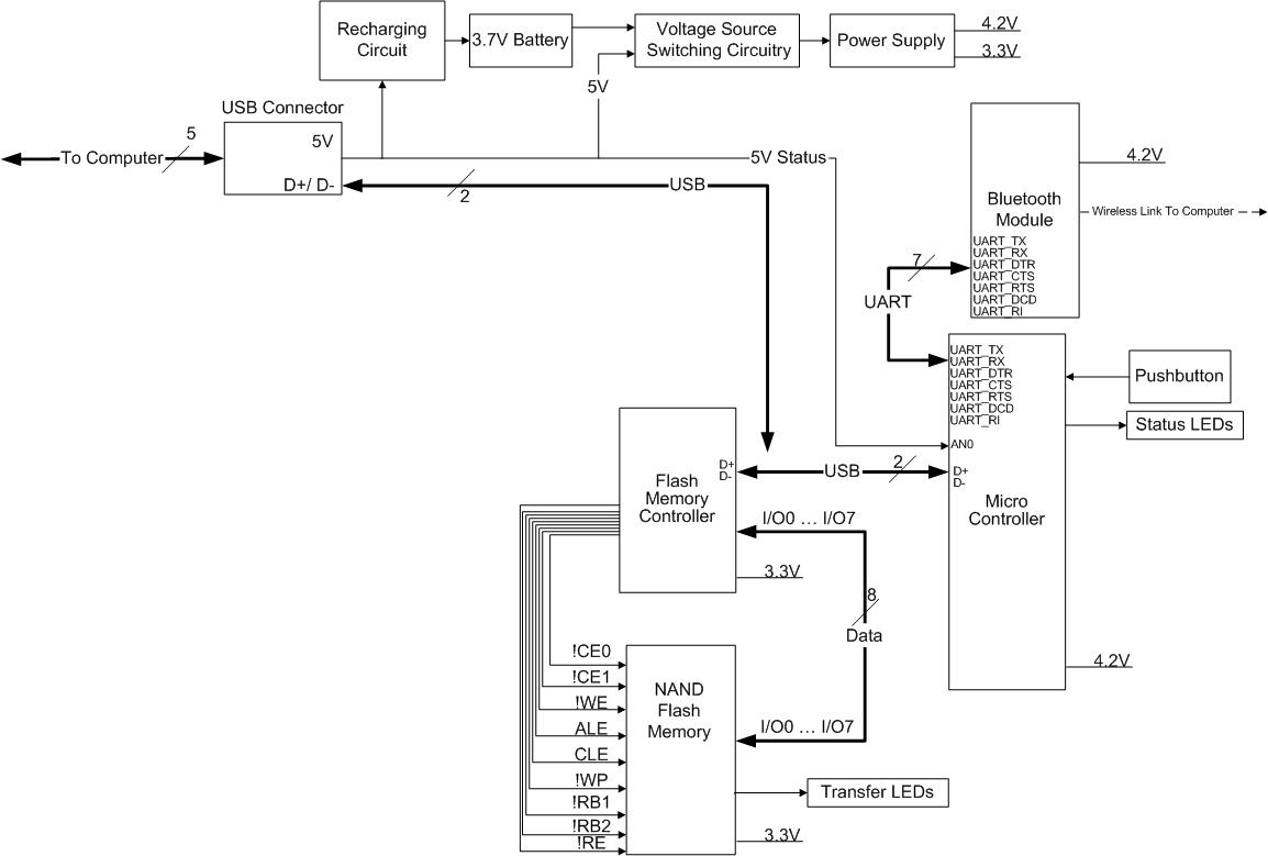
The voltage of the microcontroller had to increase from 3.3V to 4.2V because we need an increase in clock speed so we can manage the file system on the NAND Flash and
transfer data from the NAND Flash through the microcontroller and to the Bluetooth module. The reason for doing this is to tranfer data from the USB differential lines
and change it to be transfered to the module via UART.
After seeing Group 5's TSCP today there was some interest in the MAX3301E USB On-the-Go chip among are group.
I researched the device and found the following:
The MAX3301E allows mobile devices such as PDAs, cellular phones, and digital cameras
to interface directly with USB peripherals and each other without the need of a host PC.
It supports USB 2.0.
The IC has a UART Mode where D+ transfers data to DAT_VP and SE0_VM transfers data to D- in UART mode. D+ and D- goes through a level translator to be used at various voltage levels.
SE0_VM is System-Side Data Input/Output. SE0_VM is an input if OE/INT is logic 0.
SE0_VM is an output if OE/INT is logic 1. DAT_VP is System-Side Data Input/Output. DAT_VP is an input if OE/INT is logic 0.
DAT_VP is an output if OE/INT is logic 1.
with the dat_se0 bit
I also researched how the NAND Flash controller actually works (before we saw it as a "Black Box"), and found
Micron's NAND101 Tutorial . It is very helpful in gving insight on how to control
NAND Flash. It also provides referenes to NAND Flash, Managed Flash, and Flash Controllers. From this tutorial I found a very inclusive microprosser for our device.
The i.MX21
from Freescale is a processor that manages Flash, USB and Bluetooth, but also as very uncessary periphars. However, these can be turned off so power consumption
can be kept minimal as needed from our design constraints. I went ahead and ordered a sample just to have if our previous modulated idea becomes unfeasible.
A 8 GB NAND Flash IC from Micron was found, and can be bought. The only issue is there is no readily available datasheet.
However, this has been requested and we are waiting for the datasheet before we buy the part. From the previously mentioned NAND 101 controller, all NAND Flash is inherently the same (i.e. most chips
can be swapped out without chaninging the USB design.) Therefore, if it is the wrong part our schematic and PCB designs will ultimatley remain unchanged.
February 14, 2008 (6 hours): We met as a group to discuss further discuss the microcontroller's increasing role in our design.
Orginally, we were trying to lighten the load on the microcontroller, but now we are using the microcontroller to manage the file system on the device and
communicate accordingly with the Bluetooth Module. The FTP protocol was also discussed and this may be problematic due to its reliance on having software stored the computer.
I contacted a Micron sales office to try and find some datasheets for their Flash devices that are in stock. The primary oscillator of the PIC will be run
at 48 MHz for USB and cannot be used for any other peripherals. This leads us to designing the secondary oscillator Section 12.3 of the PIC datasheet
gives some guidelines for this. The block diagram was also updated to allow for the new 4.2V rail that is needed by the PIC now running at 48MHz:
February 15, 2008 (1 hours): I reviewed the Theory of Operation and Hardware Design Narrative homework
and commented the document with any changes and concerns I had.
February 16, 2008 (12 hours): I reviewed the Motorola AN1259.pdf on the homework page and datasheets of our major components and compiled a list of all special design constraints
that have to be considered when designing our PCB layout. The full list can be seen in PCB_coniderations_outline.doc .
While looking over the schematics I found a critical error in the DC to DC part selection.
The MAX1797 that had been chosen had a minimum steady state current of 400 mA with a typical current of 550mA.
However, powered USB hubs provide 500mA current maximum. The MAX1796 from the same family of DC to DC converters
has a typical steady state current of 300mA with a current limit of 500mA. The MAX1796 has been ordered and has
the same design requirements as the MAX1797 so no further design changes are needed.
WEEK 06 SUMMARY
Accomplishments: Theory of Operation and Hardware Design Narrative, Preliminary Schematic Drawing, and Preliminary Bluetooth programming.
The PCB design constraints were reviewed and pulled from the datasheets of the major components.
Weekly Work Total: 31 hours
Project Work Total: 82 hours
February 17, 2008(10 hours): I finished researching the design constraints of the major components of our system
the finished document can be seen here . Note: this document is just an outline for the report and has comments
to help the designing of the PCB and is not professionally formatted.
I worked with Yuri to intensely review the schematic. Bulk capacitors and decoupling capacitors were already included in the circuit and were further discussed.
There is still a question if we need a bulk and decouopling capacitor at the +5V line entering the circuit from the USB connector. The following things were changed:
Power Supply
Another switching inductor and capacitor were added so they were not shared between the two DC to DC converters. Sharing the switching circutitry would have resulted
in less than optimal behavior.
Bluetooth Modue
The schematic was changed to reflect the updated firmware that changed some of the pins. All of the signals but the PCM related ones are being pulled to headers for
potential future use and debugging. PCM was not used bcause we are not using the audio codec on the Bluetooth module is not needed for our desing.
Microcontroller
One of the status LEDs was removed. It is not needed and would have drawn to much power. To show different modes we are going to pulse the LED at different rates.
Some questions that need to be answered are where decoupling capacitors need to be for the microcontroller and their values.
We are planning to use the USB +5V to interrupt the circuit to turn off Bluetooth Module. Special care is being taken to protect this interrupt as well as the reset line.
Also, to power off the module commands are going to be sent over UART to turn on and off the device. Scott is supposed to investigate this and do some power mode
experimentation to see if external circuitry is needed. A voltage divider circuit was added to limit the voltage into the terminal to fit the specifications of being within 0.3V of Vdd (min of 3.0V max of 3.6V).
Several other questions arose from the USB developers guidelines. The following paragraph needs to be investigated further:
"Use the following termination guidelines:
1. High-speed USB designs require parallel termination at both the transmitter and receiver. For host
controller designs that use external termination resistors, place the termination resistors as close as
possible to the host controller signal pins. Recommend less than 200 mils if possible. Follow the
manufacturer�s recommendation for the termination value needed to obtain the required 45 ohm-toground
parallel HS termination.
2. For downstream ports, a 15 k-ohm pull down resistor on the connector side of the termination is required
for device connection detection purposes. Note that this pull down might be integrated into the host
controller silicon. Follow the manufacturer�s recommendation for the specific part used."
Oscillators
The oscillator circuitry was examined. It was found that two external clocks for the microcontroller were not needed and the interal clock of the microcontroller will be running at
48 MHz. Crystals were found. One clock needs to run at 48 MHz for the microcontroller and another clock needs to run at 24 MHz
for the Flash Controller. The high-frequency filtering capacitor values depend on the crystal manufacurer, but Yuri and I are unsure how to calculate these values and are going to office hours Monday to get further help.
Flash Controller and Flash Memory
The Flash Controller calls for analog ground as well as digital ground. We think that analog ground should be used to sheild the clock and the USB differential pairs, since
there are pins for analog ground next to both of these. Digital signals are not to pass over the analog ground plane and vice versa. All of this needs to be considered for our PCB design.
After making the necessary changes above and that are also depicted in Yuri's notebook we began to run the DRC on the schematic in Caputre.
Several errors were found and corrected. All of the pins on the parts we created had to be named different (i.e. GRND1, GRND2, etc). The
pins were labeled sequentially to get the DRC to complete without errors. A netlist was created and we started to create the footprints of the major components.
February 18, 2008 (12 hours): I contaced Cypress to find some compatible NAND Flash Memory and the sent the Compatibility List . All of these
maufacturers on the list were contacted. Most of the distributors were out of stock or only took large orders ($100-$500 minimum). I am still awaiting a response from Samsung and Toshiba for samples.
I made footprints for all of the parts for our PCB layout. Most of these footprints had to be made from scratch and took some significant time as the laearning curve had to be climbed as well.
February 19, 2008 (12 hours): I contaced Micron about the T29F2G08A30A 2GB NAND Flash Memory. The product is discontinued, and the sales
representive is trying to find some parts for us to sample. For the Toshiba parts I recieved the following in response to an inquiry email:
Unfortunately all these parts are discontinued and no longer available.
Toshiba has issued an EOL(end of life) support for all SLC( single level
cell) Nand Flash cards. Currently Toshiba is pursuing the consumer markets
as well as the memory cards markets with the MLC (multi level cell) which
has an erase/program endurance of <10,000 cycles but a very high density
of up to 16Gb.
Hynix has provided us with datasheets of several compatible NAND Flash Memories. I plan to contact the local sales represitive tommorow about odering samples.
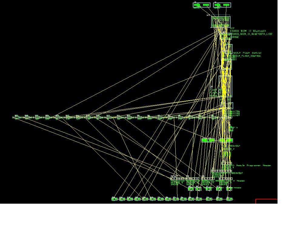
I finished creating all of the necessary footprints. ECO was ran, and the rubber-bad diagram was created and can be seen below:
The team met together and we all learned how to move the components around the board, so we can each work on the layout when we can. I finished the TCSP for tommorow, and began to
write the report that is due Friday. The presentation can be seen by clicking the link on the homepage, and the homeowork will be posted upon completion.
February 20, 2008 (8 hours): I contaced Hynix for compatible Flash memory. They were not willing to sell or sample us the part needed.
I contacted Chuck to see if he has any ideas were we can find some compatible flash as I have exhausted all of my ideas.
There is a question about the decoupling capacitors that are needed by our Flash Controller. The data sheet does not specify these values nor tell how many we need.
There are 6 digital VCC inputs and 2 analog VCC inputs.
The layout was continued. The final footprint layout was decided and the tracing layout was started and will be finished tommorow for our first "finalized" version of our board.
I contiued working on the homeowork due Friday.
February 21, 2008 (11 hours): I finished working on the report and sent it to the other team members for a quick peer review. I finally found a distributor the
NAND Flash Memory (Part Number: NAND01GW3B2BN6E). The problem originated when the compatiblity list
that Cypress supplied was out of date, so all of the part numbers were either discontinued or not correct. Yuri is calling Arrow tommorow, whom I already talked to,
to place the order. We are placing an order Monday with Mouser for the rest of our components. We are odering enough for 2 protoboards and 1 PCB.
Yuri and I did the PCB layout for the rest of the night. A picture of the first finalzied layout can be seen on his notebook. For the Flash controller pads for the decoupling and filter capacitors
February 23, 2008 (7 hours): I met with Yuri to update the schematic and PCB. After completing our first revision of the schematic we realized we could optimize
some of the general purpose I/O of the microprocessor. The voltage refernces in capture were also change to off-page flags becasue Layout Plus could not recognize the connections as the
same net. We added the HIROSE connector (DF12(3.5)-40DP-0.5V(86)) to the order we plan to make Sunday night or Monday.
The HIROSE connector is found on Digikey, but not on Mouser. The NAND Flash was not ordered and they were closed when I was availabe to place the order Friday and Saturday. The order will
have to be placed by myself on Monday.
There were numerous errors for our "first final revison" of the PCB layout. Most of the errors were located in the footrpint in layers that are not critical in the design, but are for the
Layout Plus program to work correctly. Some common errors and solutions included:
Pad Spacing Error: Solutions include making sure nothing is touching the pad including text and obstacles on other layers. Note: the footprint in the library may have to be changed.
Trace width: First try chaning the segment that is highlight to the desired width. If this does not work, try redrawing the entire trace with the
desired width.
Bad pad exit: First try editng the segment that is exiting the pad. If that does not work, then rerun the trace so that it comes staight out of the center of the pad or at a right angle to the pad. Changing
the route grid to a higher number (i.e. lower resolution) helps making this line straight. I am still trying to figure out the solution to this problem if redrawing the trace
does not get rid of the error.
Off grid via: Try moving the via and placing it in another location. If that does not rid the error, Unrouting the trace and deleting the via, then redoing the trace with a new via.
Insufficient space on plane layer: The drilling is too close to the pad or trace. Redo the hole or move the hole if too close to another trace.
For some other common problems w/ solutions with Layout Plus go to HELP->Know Problems and Solutions in the Layout Plus window.
WEEK 07 SUMMARY
Accomplishments: The Printed Circuit Board Layout Narrative and Preliminary PCB Layout were finished.
NAND Flash memory was found and the rest of our needed parts were identified.
Weekly Work Total: 60 hours
Project Work Total: 142 hours
February 24, 2008(6 hours):
I reviewed what needs to be done for the formal review. I also worked on redoing the PCB layout. We also met
as a team to discuss who will do what parts for the Formal Review. I will be doing the Brief Overview, the Flash schematic and PCB, and the Block Diagram parts. I continued working on the PCB layout with Yuri to
try and finish our second revision before the Formal Review on Tuesday. There was a random text spacing error that took us awhile to figure out. It was a corrupt .max file. We ended up
starting from scratch. However, it should go much quicker now that we know the software well. All the components were placed in near identical locations as the preliminary verison.
February 25, 2008(11 hours):
The NAND Flash Memory (Part Number: NAND01GW3B2BN6E) was ordered from Arrow and should arrive by Friday.
I worked with Yuri in redoing the PCB layout. Some of the locations of parts was changed as well as the majority of the routing. A overall schematic was created to show all of the compents of the design
on one page. A picture of it is located below:
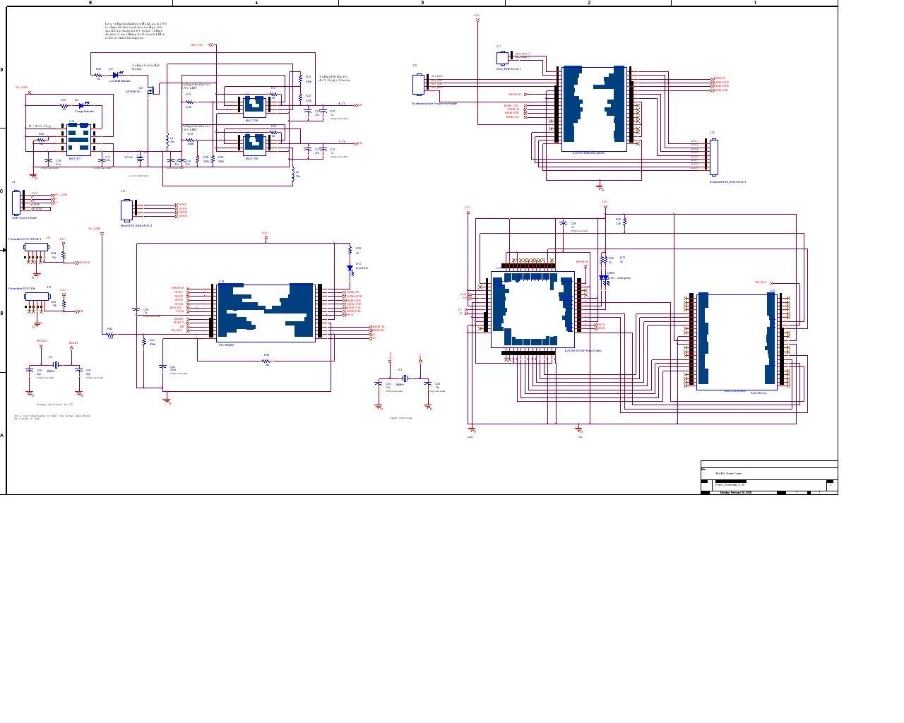
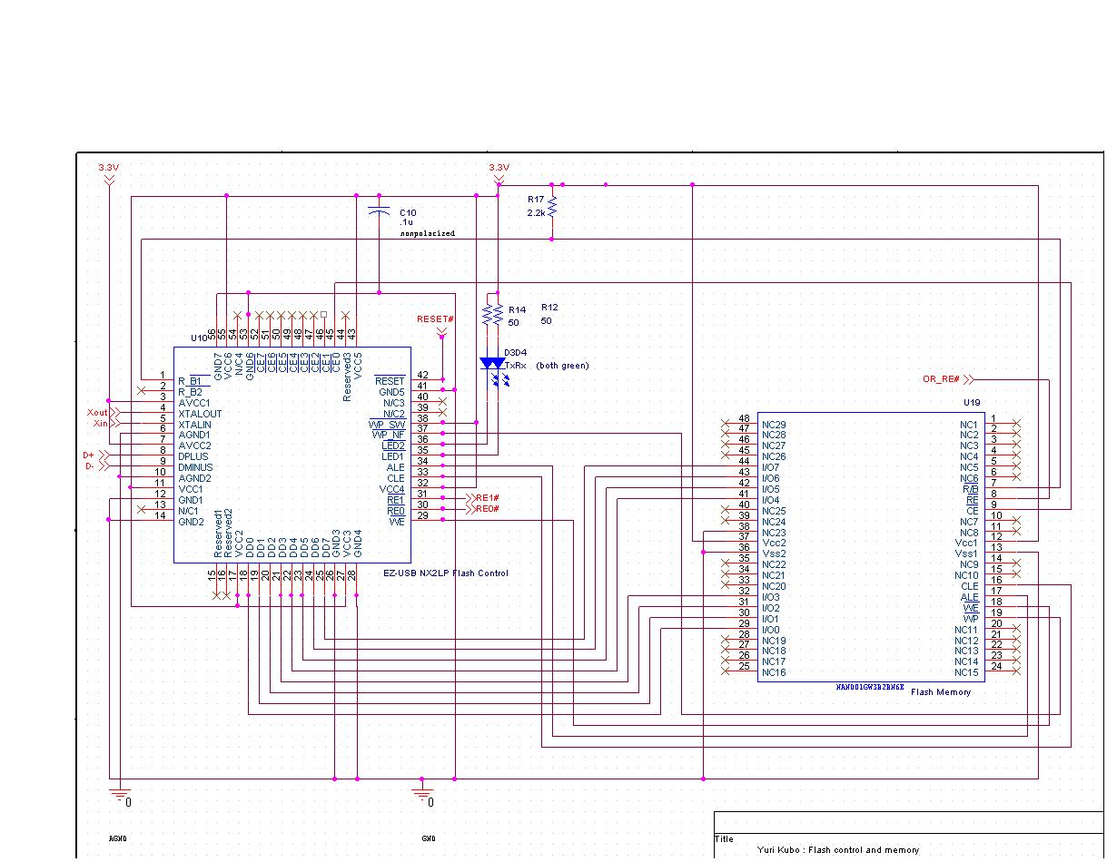
The pin layout and footprint of the ordered flash memory was verified against those in the schematic and PCB layout. The new schematic for the flash memory can be seen below as well:
I worked on my section of the formal review and has a team we practiced the presentation.
February 24, 2008(4 hours):
I met with Yuri to finish rev 3 of the PCB. I also created an order list for Mouser and Digi-key.
Below are some pertinent comments from our Formal Review:
Schematic/Theory of Operation:
cap symbols, LED current limit resistors - values could be larger for less power dissipation
check RE0/RE1 interface (4.2 vs 3.3)
2.) Project-Specific Success Criteria: 1 x 9 = 9 pts.
"Connect to" doesn't quite say what you will really demonstrate.
3.) Block Diagram:
most of block diagram is missing from handout
4.) Component Selection Rationale:
What alternative components were considered, especially for the most expensive or complex parts. Small quantity availability is understandable as reason for choice for prototype, but what would best parts be for production?
Component selection slides don't identify the actual parts selected.
6.) Schematic/Theory of Operation:
What is the expected battery life & how did you determine this?
Is low batt LED on continuously?
I suggest strobing the LED and perhaps having it be a power rather than low battery indicator.
Are all the different chip resets compatible with each other?
Suggest at least cap on reset or better yet, a reset controller.
Make sure voltage levels between chips are compatible.
MOSFET part number missing.
7.) PCB Layout:
not quite ready. Turn off all but traces and component outlines on layout so it is easier to see what is going on.
8.) Preliminary Software Design:
ok overview of what is to be implemented, but lacking detail. A block diagram or flow chart would be helpful to clarify the intended operation of the software.
9.) Project Completion Timeline:
not enough task breakdown for timeline to be meaningful
We plan to make the suggested changes to our schematic and PCB.
WEEK 08 SUMMARY
Accomplishments: Formal Design Review
Weekly Work Total: 21 hours
Project Work Total: 163 hours
March 3, 2008(6 hours):
We met as a team to discuss chaning out microcontroller. We decided to change our microcontroller to
the CY7C67300. With this new circuitry will have to be added
and a majority of the old circutiry will change. External EEPROM and SRAM were also chosen for the new microcontroller.
An external 12 MHz clock was also be chosen. I created the footprints for the new parts. They are in the newly updated library. I discussed with Yuri the new design constraints
of adding the new parts. Logic levels need to be considered; the voltage sources were also changed from 4.2V to 5V for the micro. I also changed the capture libraries for the new
componets that we are now going to use. This includes the new microcontroller, EEPROM, and SRAM.
March 4, 2008(6 hours):
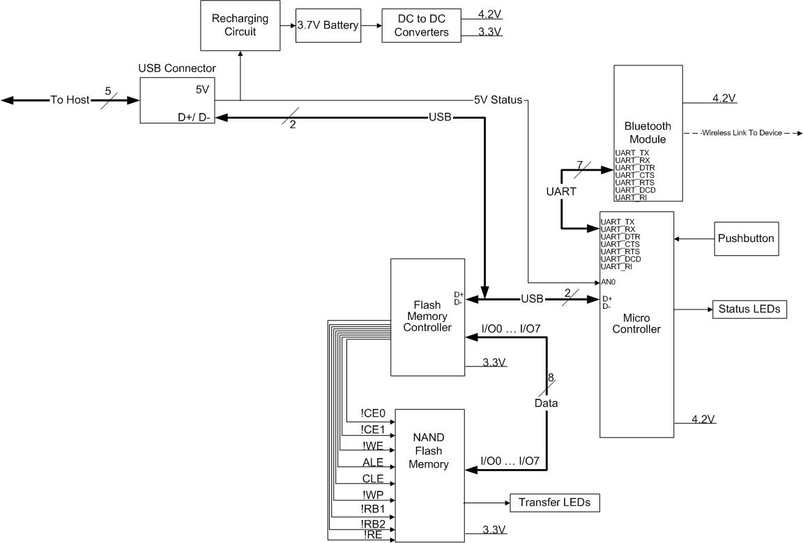
I updated the block diagram for the new parts ordered. One of the voltage rails changed from 4.2V to 5.0V.
The flash memory and controller interface was also updated per the new memory. The updates can be seen below:
I worked with Yuri and Scott on solving several problems with programming the microcontroller and EEPROM
if it was on our PCB board. These issues are still beign discussed. The reset controller was found. I choose the MAX811 based on its low input current and lack of extrnal componetry.
It has been prdered from Maxim and is being shipped. I created a footprint for the MAX811 for the PCB Layout. I also created a footprint for the new faster SRAM.
Iworked with Scott and Yucel to see if all of the footprints matched the parts we have on hand 1:1. We took in consideration extra pad space so we could easily solder the device. The EEPROM, SRAM, NAND Flash, and crystals still need to be verified.
I worked with Yuri to determine what pins we need to connect to the microcontroller and what pins to connect to headers for future use. We used the older schematic as a reference to double check any discrepencies we may have had.
March 5, 2008(7 hours):
After meeting for the progress briefing we met as a team to discuss whate we have to be done today to make sure we can have our PCB ordered before
Friday. I updated the footprints according to the parts we have and changed the NAND Flash footprint to allow for space in soldering. We decided to change the USB port on our device from a
male to a female. The new USB Receptacle will be ordered from Digikey later today.
I updated the footprint for the USB recpetacle and it is now in the new PCB layout.
I worked with Yucel in finding smaller crystals for our oscillator circuits.The following our parts (with links to Digikey) that need to be ordered inculding the smaller
crystals, USB recptacle, and Hirose connector:
12 Mhz Crystal: order 4
24 Mhz Crystal: order 4
Hirose Connector: order 4
Reset push button: order 3
USB recpetacle: order 3
The EEPROM and back-up EEPROM that we planned to use are not compatible with the Dataman-48LV, which is the only way we can feasibly program the EEPROM. Here is
a Dataman-48 LV Compatiblitiy List that we are using to find compatible
EEPROM. I found the 24AA256 from Micorchip. This is 256K EEPROM that is compatible with the Dataman. Here is the refernce page for the 24AA256 EEPROM.
I put in a sample request for the illuminated pushbutton we plan to use for the user to select modes of operation for our device. I order samples from Schurterand NKK Switches.
We found a reset pushbutton in lab, so the above link is invalid at this time. A new footprint was made and the new pushbutton is the the layout.
WEEK 09 SUMMARY
Accomplishments: Progress Breifing, Finalized Schematic and PCB Layout, ordered the last of the neede parts.
Weekly Work Total: 19 hours
Project Work Total: 182 hours
WEEK 10 SUMMARY
Accomplishments: Spring Break!
Weekly Work Total: 0 hours
Project Work Total: 182 hours
March 18, 2008(2 hours):
I met with Yuri to discuss the progress that had been made since I was on my interviews before
and after Spring Break. We picked up the PCB and looked it over for any defects in manufacutring. No defects were found. Shorts between power and ground were
also looked for by checking continuity. None were found. The reset controller, EEPROM, and Pushbuttons all arrived and were put with the other components.
I emailed a EET professor about reflow questions that we have.
March 19, 2008(5 hours):
The EET professor wants to meet with us so he can see our PCB. Yuri or I will meet with him tommorrow. I printed out the PCB layout and schematic and
double-checked all connections to try and see if there are any errors.
March 20, 2008(2 hour):
The EET professor recommened that hand solder what we can either with the soldering iron or with soldering paste and heat. Either Yuri or myself are going to
go and check out the EET surface mount lab as the solder paste and heating gun are not available to us in the Senior Design Lab. He recommened populating the larger
components first and saving the Flash controller for one of the last things since it is the hardest and the IC most subject to error. For the large memory
ICs on the bottom of the board we will have to use an epoxy substance to hold the ICs on the board if we choose to use heat and solder paste. The surface tension
of solder is great enough to hold on the smaller parts, but not the fine pitch memory ICs. I continued checking for errors on the PCB by lookingat the printout. This
was a bit of a challenge since I did not have software on the tablet. However, I beleive that all of the traces are correct and not nets are connected together that should not be.
March 21, 2008(1 hours):
I finished checking to make sure all of the pins were connected to the right traces and verified the pins of the ICs to their respective datasheets. All ICs look correct.
March 22, 2008(4 hours):
I updated all of the links on the datasheets page. This will allow quick and easy reference of all datasheets used in our design. Yuri and I debugged the power supply
that has been populated on the PCB. The 3.3V rail is outputing 3.7V. The 5.0V rail is outputing the correct voltage, but is still outputting 15 mA of current
when it is below the cut-off voltage. I contacted Cypress about the problem and am currently awaiting their technical support.
WEEK 11 SUMMARY
Accomplishments: Checked PCB layout for errors and began populating the PCB. Software development has also been started.
Weekly Work Total: 14 hours
Project Work Total: 196 hours
March 24, 2008(2 hours):
I worked individually on the Patent Liability Analysis report and presentation. I found several products and patents that are close in functionality to our design.
March 25, 2008(7 hours):
I met with Yuri to find out the status of the project since I have been doing a significant amount of traveling for interviews. We went to the lab and looked at the 3.3V rail
as the input voltage changed. Our results can be seen here. The resitance load was chosen to obtain a current of aroun 250mA and then changed to several different values for comparison.
For input voltages above 3.6V the output voltage is 0.2V below the input voltage. For voltages below 3.6V to the cutoff voltage the output voltage is close to the 3.3V desired. The primary concern is with
applying a voltage greater than 3.6V may cause some of our IC's, espicially our microcontroller, to function erratically.
I continued working on the Patent Liability Analysis report. Yuri will be doing my TCSP tomorrow, since I will be in Washington DC for another job interview. I will do
his TSCP next week. I made the slides for the TSCP and went over them with Yuri. The presentation can be found on the presentations page of our site.
March 26, 2008(2 hours):
I continued working on the Patent Liability Analysis report. The three patents that I choose are the following:
United States Patent: 6795327. Inventors: Deng, Guoshun, Cheng; Xiaohua, Xiang; Feng.
United States Patent: 6874044. Inventors: Chou; Horng-Yee, See; Sun-Teck, Chu; Tzu-Yih.
United States Patent: 20030216954. Inventor: Buzzelli, David B.
I also consulted with Yuri via a phone call about the power supply. He ran a couple of work arounds by me. Please see his notebook for the specifics. The basic idea is the dc-to-dc converter for the 3.3V rail
is not a step-down converter (only a step-up). For voltages above 3.6V it would likely destroy the 3.3V supplied parts.
March 27, 2008(7 hours):
I finished the majority of the report. I consulted with Yuri about the power supply issue again.
The resistor did not work, and he came up with a solution using a power MOSFET. I thought it would be worth a try to try the idea. Please see his notebook
for the details.
March 28, 2008(13 hours):
I completed homework 10 and submitted it after using some of Yuri's suggestions. It is also posted on our website.
Yuri and I went to the EET Surface Mount lab to meet with a EET professor and learn the necessary soldering techniques
to populate our board with fine pitch devices. We are using a solder paste dispenser with a hot air to popluate the fine pitch ICs.
Using the solder paste dispenser one can use two different techniques in dispensing the solder paste. One uses a thin line and the other uses a small dab.
The thin line will be used for the finer pitched parts and the small dabs can be used for larger components. The hot air blower is used to heat the paste.
The paste is made of solder, flux, and a mix of material to make the paste consistent. If one heats up the paste too fast the paste will evaporate too quickly
causing bits of metal to "explode" across the board. We also learned how to use a manual part place machine. It uses a vaccuum to
suck up a part so one can corretcly orient the part and place it on the board.
Some problems that we ran into with the small pitch ICs are the pads on the PCB are placed underneath the device. This was done orginally
to aid in the soldering process, but may have hindered it. The work around for this was using an exact knife to keep
the heated solder from bridging.
On the Hirose connector GPIO 5 and 6 are bridged. Also, USB1 is shorted to GND4. The GPIO's are not being used and the USB1 is not used. The issue is
whether USB1 can be connected to ground when it is not connected. These bridging issues were fixed. The componets for the 3.3V rail were removed as
that power supply is being changed. The HIROSE connector, the NAND flash IC, and the microcontroller have been placed on the PCB.
The rest of the board will be populated Sunday. We met as a team and discussed our progress. I helped Yuri with populating the microcontroller
section of the board.
The packaging needs to be ordered. It is a external hard drive
enclosure. The case is clear for asthetics. There is a inside PCB board that will have to be removed.
March 29, 2008(7 hours):
I met with Yuri to see what parts needed to be ordered. I updated the Bill of Materials (BOM) and sampled more parts, so we will have enough to finish our design with extra components
in case of damage to them. I also put together a list of parts to be ordered from Mouser. I updated the datasheets page to include the MAX710, the DC-to-DC up/down converter. I created the new footprint for the MAX710 and the Schottky Diode.
Before placing the order I tookinventory of all of our parts to amke sure we are buying the correct amount of components. The inventory can be found on the second tab of the the Updated BOM . The order should be placed tomorrow.
WEEK 12 SUMMARY
Accomplishments: I worked on the Patent Liabiltiy Analysis report and presentation. We began the populating the PCB using surface mount
techniques. The rest of our parts were ordered or sampled. The software design was also continued.
Weekly Work Total: 38 hours
Project Work Total: 234 hours
March 30, 2008(11 hours):
The MAX710 and CY7C67300-100AXE microcontroller have been shipped. The Updated Bill of Materials (BOM) was used to place an order for more electronic components.
The following changes were made to the schematic:
A 5V USB indication line to the microcontroller. This was done using a MOSFET as a voltage level translator. This signal is from the USB header and can be used to send a message to the computer letting the user know the device is plugged in.
The SPI signals from the microcontroller were named MOSI, MISO, SCK, nSSI. These signals were already sent to headers M_GPIO7...M_GPIO4.
The Updated Power Schematic
The Microcontroller Schematic
I went with Yuri to the EET Surface Mount Lab to populate the majority of the rest of the board. Here is an application note from Silicon Labs with some recomended techniques in soldering and desoldering fine pitch devices. After we populated the board, we met as a team to discuss the new design
changes and everyone looked over the changes to the schematic and layout to make sure they were correct and no further changes need to be made.
We met together as a group to see where the hardware and software portions of our project are currently standing. The PCB board has been fully populated and the new parts have been ordered.
The changes to the PCB layout and schematics were discussed and a couple minor issues were found and corrected. We went to the lab to test the board. The board powered up
after a few changes to circum-navigate the non-exsitent 3.3V rail. There was an issue with a broken oscilloscope probe.
It should a 60 Hz signal even when probing a DC power supply directly. To find the issue we had to remove the crystal from the flash controller, but it was repopulated after the
broken probe was found to be the cause of the issue. Both crystals are operating to their respective specifiations (12 MHz and 24 MHZ) and critcal signals are mostly noise-free.
March 31, 2008(6 hours):
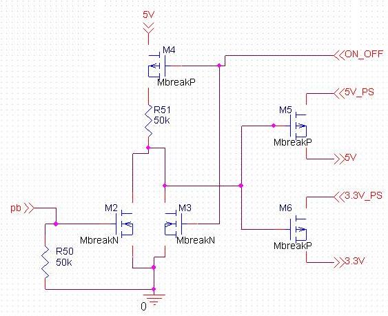
I met with Yuri to discuss the pressing hardware issues. Yuri came up with a hardware
solution in turing on and off our device through the mode select button. Please see his notebook for the details, but the general idea is that when the
button is pressed for greater than 3 seconds the microcontroller will assert a signal to turn on or off the device by connecting or disconnnecting
the voltage rails.
I emailed the manufacture of our packaging solution to obtain the exact internal dimensions of the external hard drive enclosure
we plan to use. This is critcally important because if our PCB is too large a new packaging solution will have to be found. Pending the PCB will fit inside the enclosure, the package
will be purchased.
We were able to supply the PCB with 5V from the USB header, thus satisfying the PSSC that states charging a Lithium-Ion battery via
a USB port.
I looked for componets for Yuri's power-on/power-off circuit. It looks like using individual FETs instead of finding a switching component will be a better choice. This is because of the on resitance of the devices.
If the on resitance is not extremly low, then the voltage drop across the device causes the voltage rail to the entire circuit to drop significantly.
April 1, 2008(3 hours):
I helped Yuri with the report and presentation. I will be giving the presentation tomorrow, since Yuri covered for me last week. The presentation has been completed and posted on
the presentations page of our site.
All of the samples that have been ordered from Maxim, Cypress, and Microchip have shipped and should be in our days by the end of the week. We should have enough major components for the rest of the semester
even considering extras in-case of failur or loss.
April 2, 2008(4 hours):
The Cypress microcontrollers have been recieved. We now have eight microcontrollers at our disposal. I attempted
to tile our new PCB, but found the process to be too complicated so Chuck's assitance was requested instead. Yuri and I plan to test the flash controller and NAND Flash
cicuit this evening. I recieved a development board from Chuck for the NAND flash. We are still trying to find a development board for the flash controller. We a simple diagram showing how
we plan to test the flash controller and NAND flash can be seen below:

The D+/D- pair is supposedly sensitive to noise, so we plan to directly connect to a flash drive and , eventually, our flash controller. A power issue then arises.
Both devices need power, so we plan to use headers and solder directly to the power and ground pin, while keeping in mind to tie together the grounds. Problems with testing include not using a host computer, so our device has to be the host,
not using drivers that may be needed if communication with computer (how do we intialize the handshaking procedure). If this works we will better understand
the USB protocol and how our device needs to behave when transfering data over Bluetooth as well as the USB port. I helpe
We are also looking for FETs to test the logic of the power button circuit. We are wanting to test the logic before our new PCB is ordered.
April 3, 2008(1 hour):
I looked over Yuri's homework and gave him some feedback on the report before he turns it in.
WEEK 13 SUMMARY
Accomplishments:
The PCB was completly populated. The layout and schematics were changed according to some early testing. The parts that were
ordered arrived. The software development continued.
Weekly Work Total: 25 hours
Project Work Total: 258 hours
April 6, 2008(6 hours):
Yuri and I discussed the SRAM issues Scott and Yucel have been having. I went over the datasheets for both the SRAM and microcontroller.
From the SRAM datasheet:
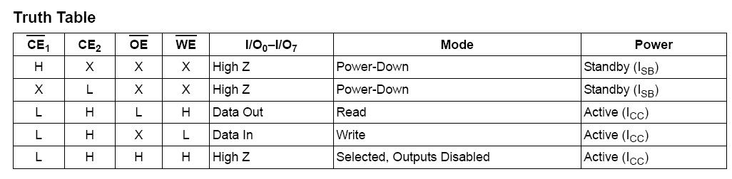
In our current design CE2 is always hight because it is pulled to the 3.3V rail, so it is always high and CE1 is controlled from the microcontroller's nXMEMSEL pin. This allows to the microcontroller to read, write, and powerdown the
SRAM with only one CE. The External Memory Control Register needs to looked at with Scott and Yucel.
The issue for the SRAM was investigated. The problem seems to be nXMEMSEL, nRAMSEL, and nROMSEL all enable different parts of memeory.
Since we are always enabling the SRAM by hard-wiring it to GND, means the microcontroller cannot access neccesarry parts of its memory. To fix this we need to use all of the memory selects. Currently the nRAMSEL and NROMSEL are no connects and not broken out to headers.
A fly-wire could be a possible solution, but would be hard to accomplish beacuse of the 0.5mm spacing of our components.
April 7, 2008(6 hours):
I read through some of the information that Scott had on our microcontroller and found a
schematic to a development board using our microcontroller. This design is
expanding its memory using SRAM. It is the output of AND-ing the nxRAMSEL and nxROMSEL to drive the nCE for the SRAM using the M74VHC1GT08DFT1G.
It can be bought at Mouser here.
It was decided that using this method to drive the SRAM's chip enable may solve our SRAM problems, so it will be implemented in the final PCB design and schematics.
April 8, 2008(8 hours):
I updated the schematic to reflect the changes made to the chip enable line for the SRAM and the On/Off button control.
For SRAM's chip enable nxRAMSEL and nxROMSEL are being logically anded and sent to the chip enable of the SRAM. nxMEMSEL is being brought to a header for future use if needed. The On/OFF button schmeatic can be seen below. The On/Off control
line is coming from the microcontroller.
The theory of ANDing the nxRAMSEL and nxROMSEL lines was tried using a PLD. This was done to test our theory as Chuck is tiling the boards.
I found some enclosures and will try and sample them tomorrow. We are going to try and cut away the lid and put on our own
clear lid. The SRAM issue was investigated in further detail. The AND gate seems to let the microcontroller read and write to the SRAM, but the results are
not stable. This may be an issue with the external memory or the code itself.
April 9, 2008(5 hours):
The packaging previously stated was sampled from Polycase. The package is slightly larger than we need, but still maintains
its portable nature. The package is not clear but does have removalbe peices, so we can put in Plex-glass peices if desired.
The microcontroller is still having issues in adressing and reading from external memory. Scott and I worked on filling up different arrays that
spread into different parts of external memory, and then we would read the contents of this memory and turn on LEDs accordingly. We were able to read and address the first
part of external memory, but not all of it. We are unsure why this is as we should be able to directly address the majority of external memory. The logical
analyzer appears to show us that everything is being read and written correctly, but we did not have the full address and data lines connected to it.
April 10, 2008(10 hours):
The full data bus and half of the address bus at a time will be hooked to real-time logic analyzer. This
will allow us to see the bytes as they are being written and read. Then, we can use the other logic analyzer for precise rise and fall times. Below is a picture
of our testing setup for the logic analayzer.
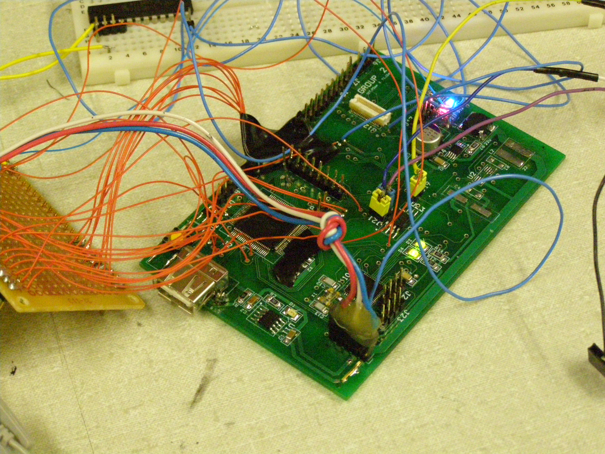
Being able to see the address and data buses proved useful in debugging the issues
with the SRAM. We were able to write and read to the SRAM, but the lowest bit of the address was staying high due to a incorrectly soldered pin. This was
corrected, and we could write to the correct address.
April 11, 2008(12 hours):
The SRAm is contined to be debugged. We wrote to various spots in external memory
and read from those address locations to verify the SRAM was functional. While doing this check we set all the GPIO pins low
to turn on the status LEDs. However, has we tried to write to larger adresses the GPIO would go low for only a clock cycle or two
starting when the write enable would go low. We decided to document this behavior and move on to finishing the PSSCs.
We were able to pair and connect the Bluetooth module to both a PC and a mobile phone. This fufills the PSSC for "Connect to a host via Bluetooth".
However, the reset controller is not connected to the Bluetooth module correctly. The reset on the Bluetooth module is active high, while the reset controller's
output is active low. To fix this we cut the trace so the Bluetooth module will not be able to be reset excpet for a power reset. This
does not change user functionality (only testing functionality). The Bluetooth header is also mirrored, so the footprint for the module is opposite
than desired. The module still connects to our PCB correctly, but module is close to header pins and will be extermely close to the microcontroller on our new PCB.
The software for the USB to act as a pass through for the USB header to the flash controller.
The design example we were using for the USB code on the microcontroller can be used to passthrough the differential pair
from USB. This is exactly what we want to do when the USB is directly connected to the computer, but the code involves using only a keyboard
instead of a flash drive.
April 12, 2008(7.5 hours):
We were able to connect to the Bluetooth module and send a .txt file.
This was done the following way:
1. The user intiates a connection using hyperterminal (or some other form of connecting to a COM port).
2. The Bluetooth module then hangs up and immediatley intiates a call with the host PC using the Bluetooth address of that host.
3. The user inputs the passkey so it is paired to the Bluetooth Module.
4. The user then connects to the device.
5. The user will now be able to send strings and text files to the Bluetooth module.
This is a strong stepping point to sending all file types across Bluetooth. Instead of using the Ezurio development tools, we will use our microcontroller
to hang up the connect call, save the Bluetooth address, and intiates the call to the PC. The PC will then automatically connect and files will be able
to be sent.
WEEK 14 SUMMARY
Accomplishments: Small programs were loaded onto external memory on our PCB. Intial Bluetooth connection was done
that can be used to satisfy a PSSC. Transfering text files from the Bluetooth module can also be done on the development board.
Weekly Work Total: 54.5 hours
Project Work Total: 312.5 hours
April 13, 2008(6.5 hours):
We are able to successfully connect to the Bluetooth Module using code
on the microcontroller. Pending course approval this should successfully pass the PSSC for connecting a host PC via Bluetooth. The
microntroller waits for a "RING" and saves the Bluetooth address. The microcontroller then terminates the connection and establishes
a new connection. The user can then enter a pass-key and connect to our device. Data can be sent to the device by typing into
the terminal or we can send a file over the terminal.
We have began working to fully satisfying another PSSC. The "Transferring Data via Bluetooth" PSSC is within reach. We can send file as .txt and then manually change the
file extension as needed. There is some errors if this file is large, but that is likely due to the slow baud-rate of 9600. To fufill the "Manage a file system" PSSC
the internal memory of the microcontroller will be used at first to avoid the external memory. As the software progresses it will be moved
to external memory.
April 14, 2008(7 hours):
The pacakge from Polycase arrived. It will fit our PCB with a few modifications.
There is a battery compartment that will be removed and some internal mounting pillars that will be removed. A hole for the user mode select
button will be drilled. Also the top of the case will be made clear by cutting rectangle out of the black casing and adding a clear Plex-glass sheet to see the staus LEDs and add to the asthetics.
A blue silicon boot also came to with the package to add some durabilty and asthetic design to the package.
Scott was able to manage a file system without the delete function, so I worked with him in adding the delete function. This was quickly added
and we can successfully demonstrate this file system from a Bluetooth connected host PC. File transfer was succesful with smaller text files or smaller files
converted to text (.txt). Larger files begin to be written into SRAM, and this seems to corrupt the files or lose data in these files.
April 15, 2008(8 hours):
I worked on the user manual and pending minor changes this should be finished tonight. It will be
posted onto the homework page when completed. Yuri ordered the PCBs. Apparently he did not stress the need for these board clearly enough, so we will not have the boards
until next week. We should be able to quickly populate the boards for a nice looking product instead of flywiring in our fixes to the power supply.
I worked with Yuri to populate the flash controller and NAND flash memory IC to two development boards. However, the solder paste was being refrigerated and hadto be left out for at least 5 hours.
The solder paste did not work correctly and shorted out all of our pins underneath of the ICs. Attempts to fix them proved to be useless.
Yuri and I went to look for a type A male header to type A male header USB cable or connector, but could not find one. I plan to go to Lafayette Electronic Supply Company tommorow to look for a connector.
We worked further on the issues of the SRAM. There is an issue with the timing of the read and write lines. Data is being written to the SRAM, but when reading
from the SRAM the result is not correct. In the external memory register the RAM and external memory waits were changed to several different possible combinations, but the effect
was always the same. Different files same to become incorrect as they enter the SRAM memory space.
April 16, 2008(6 hours):
We met as a team immediately after the progress briefing to attack the pressing SRAM issue. The chip
enable line was shortned. We thought the unessecary length may be causing extra noise and delay on the line. This did not prove to be a solution, so more combinations of the
wait delays were tried to no avail. When writing a file completly to SRAM the program crashes and spits out meaningless contents of memory. This consistently
happens whcih leads back to the timing being an issue.
April 17, 2008(10 hours):
Chuck had a idea to write a small program to delay the wirting and reading the SRAM. We should write
a program that writes 1K of data to the SRAM at 1ms per byte. This will take a long period of time to complete the read and write, but we should be able to elinate
noise issues from faster switching. This would also let us see if our SRAM is physically bad due to possible static shock or some other occurance.
A small check loop was written that wrote data to the SRAM and after a 1 ms delay checked it. This seemed to show that data was in fact
being read/ written correctly to/ from the SRAM, but it was later found that the data was being stored in registers on the microcontroller.
This makes since because the microcontroller tries to do the most efficient process possible. We then tried writing a 1 kB block to SRAM
and then reading these values back. This gave us back some data, but it was either incorrect or missing all together. There
may be a noise issue involved from the TX/RX lines and the Bluetooth antenna.
April 18, 2008(7 hours):
Continued debugging the SRAM. It was found that D3 was always pulled high during
the read from the microcontroller. During a write the microcontroller forces D3 low. This means that the data is being writted to SRAM, but not read correctly.
The error is most likely in the software on how we our reading and verifying data from the microcontroller. The microcontroller
is 16 bit while our SRAM is 8 bit. The microcontroller is likely handeling the 8 bit data as it would with 16 bit data.
WEEK 15 SUMMARY
Accomplishments: We can successfully connect/ disconnect to the device via Bluetooth from a host PC multiple times.
We can also successfully manage a file system via a Bluetooth connected host. Commands put, get, dir and delete all function.
Weekly Work Total: 42.5 hours
Project Work Total: 342 hours
April 20, 2008(7 hours):
I began working on the final report and looking at what changes need
to be made to our homework so they can be integrated into the final report. The SRAM has been fixed and larger files that run into SRAM
can be recovered correctly. We began working on the mass storage class code. This will allow us to communicate with the
NAND flash and is the last step in making our device fully functional.
April 21, 2008(8 hours):
We tried to check off our 4 completed PSSCs, but since our device is not
completely stand alone (the 3.3V rail is powered by a bench power supply) Karl was unable to check us off. Our PCB should be in hand by Wednesday, so with a timely
population of the board 4 of the 5 PSSCs will be checked off later in the week.
When plugging out board into a host PC via USB to charge the battery, the host PC recognized our device and we were able to see the devices ID.
This could count as compeletion for our 5th PSSC, "Connecting to a host via USB".
I brought a USB to serial converter to finish testing of his GUI. We were able to send the commands of
file transfer to another computer via a wired connection. I began looking at all of the MSC code and various functions
inside of the code.
April 22, 2008(12 hours):
I worked on my part of the final report which includes the Patent Liabilty Analysis and PCB design
considerations.
The PCBs arrived from 4PCB.com. Yuri cut them apart since they were tiled
but not cut. The power supply was populated and tested on the final board and a "fail safe board." Both the 5V and 3.3V power rails
are withing the specified voltages of 3.3V and 5V. The rest of the two boards was then populated. As Yuri was soldering one board, I would
test all connections of the major fine pitch components on the other board. I was checking for bridged and non-connected pins. After
all the errors were fixed the passive components were populated on both boards.
April 23, 2008(9 hours):
The two populated boars were tested. Both work with our code, and the 5 PSSCs were checked off.
The power on/off button was then tested and the code was written so the microcontroller can power on and off the entire board with a button press
of 2 seconds. The GUI was worked on to provide a better user interface as well as looking more profesional than using HyperTerminal. The status LEDs on teh device were also brought out of "debug mdoe" to provide better user feedback. Once these changes are completed the video will be made.
April 24, 2008(9 hours):
I worked on my portion of the Final Report and finshed the PCB considerations, Patent Liability, Abstract, Project Overiew with Block Diagram, Version 2 Changes, and Conclusion. Pending the other team members contributions the Final Report
will be posted on the site.
I worked with Scott to get the device ready for the video and out of debug mode. Then we proceeded to make our video. The camcorder we used is a harddrive camcorder and
records in .mod which is not supported by any editing software.
April 25, 2008(5 hours):
I worked on the video and tried to find a converter to convert the .mod file to a usable format. Most likely we will just
retape the video on a dv camcorder otherwise editing the video will not be possible. I worked on compling the final report by profreading Yuri's and Yucel's contributions and making necessary changes and suggestions when needed.
April 26, 2008(2 hours):
I worked on trying to get the .mod files ready to edit, but could not find a converter that worked 100%. I
proofread Scott's contribution and added it to the final report.
WEEK 16 SUMMARY
Accomplishments:The SRAM was fixed allowing for larger temporary file transfer. The new boards were popluated.
All 5 PSSCs were checked off!! The GUI was finished. The documentation that is due Monday was all but completed.
Weekly Work Total: 52 hours
Project Work Total: 394 hours
April 27, 2008(5 hours):
The video was redone and edited. The final report was compiled and the senior desing report was finished.
WEEK 17 SUMMARY
Accomplishments: The video and documentation was completed.
Weekly Work Total: 5 hours
Project Work Total: 399 hours