Trigate Gen 1
Differences from a planar DMOSFET
In a conventional planar DMOSFET, an electron inversion layer is formed on the upper surface of the p-type base implant. Electrons flow from the n+ source, across the inversion layer, into the n-type JFET region, and downward through the n- drift layer into the n+ substrate.
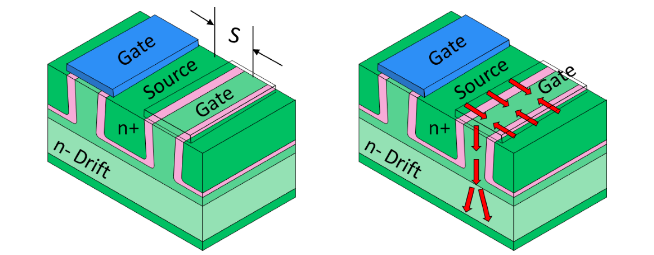
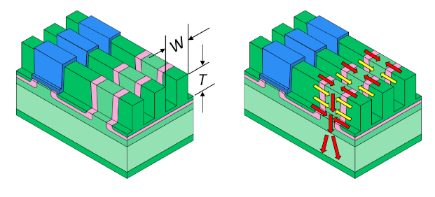
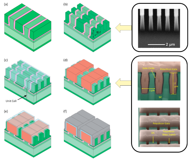
The tri-gate (3G) MOSFET is formed from a DMOSFET by etching trenches that run perpendicular to the gate and source fingers. This places a MOS gate over the sidewalls of the p-base implants, creating new channels (yellow arrows) for electrons to flow from the source to the JFET region.
Specific Channel Resistance Advantages
For a conventional DMOSFET, the specific resistance of the MOS channel is given by:
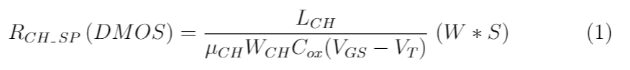
where LCH is the channel length WCH is the channel width, µCH is the inversion layer electron mobility, COX is the oxide capacitance per unit area, S is the half-pitch of the unit cell, and W is the width of the unit cell. In the DMOSFET, the channel width is the same as the unit cell width, i.e. WCH = W.
For a tri-gate MOSFET, if the trench depth is T and the unit cell width is W, the specific channel resistance is given by:
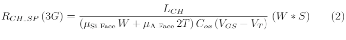
Taking the ratio of specific resistances, equation (2) / equation (1), gives:
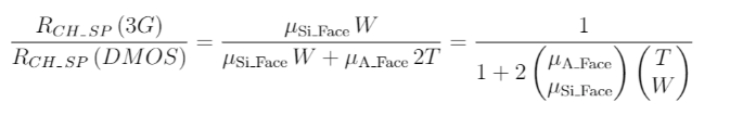
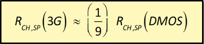
If T = 2 µm, W = 1 µm, and µA-Face = 2 µSi-Face, then:
Trigate Device Fabrication
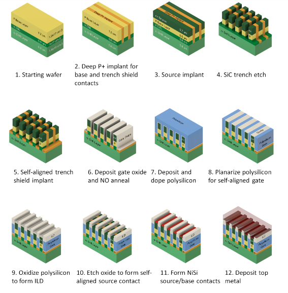
Steps in the fabrication of the 3G-MOSFET:
- Implant p-type base and n+ source regions using a self-aligned process. MeV implant energies are required.
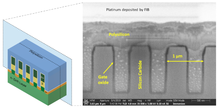
- Etch trenches perpendicular to the gate and source fingers. Trenches are ~2 µm deep and 0.5 µm wide, separated by 0.5 µm mesas.
- Deposit gate oxide and perform a post-deposition anneal in nitric oxide (NO). The basic unit cell is shown dotted.
- Deposit doped polysilicon to fill the trenches. Pattern into gate runners.
- Form a thick oxide over the polysilicon by thermal oxidation. Clear the thin oxide over the exposed SiC with a short etch.
- Deposit ohmic metal and anneal to form source and base contacts. Deposit top metal over the entire active area.
IMOSFET
Single and Double-Trench Oxide Protected MOSFETs
Silicon carbide (SiC) trench MOSFETs (UMOSFETs) exhibit lower specific on-resistance than planar DMOSFETs, due to:
- A more compact, scalable unit cell
- Higher electron mobility on a-face surfaces
Oxide electric fields should be kept below 3-4 MV/cm for long-term reliability. [1]
Critical Issue: Shielding gate oxide from high electric fields at trench bottom
In this work we provide simulation results and describe the fabrication process of IMOSFET- a deeply-scaled, fully-self-aligned trench MOSFET with a P+ trench shield implant.
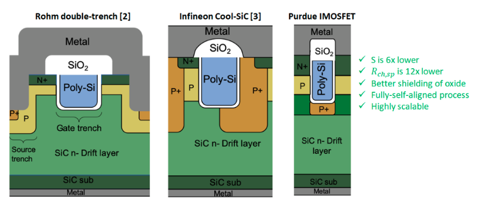
- The IMOSFET has two channels per trench, while Rohm and Infineon UMOSFETs have one channel per trench
- Rohm and Infineon UMOSFETs have continuous P+ contacts, while the IMOSFET has segmented P+ contacts
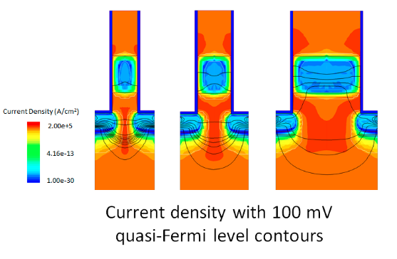
Optimization of the IMOSFET
We optimize each structure to obtain the highest figure of merit 𝑉𝐵 ^2∕𝑅𝑜𝑛,𝑠𝑝 , where 𝑉𝐵 is the blocking voltage and 𝑅𝑜𝑛,𝑠𝑝 is the specific on-resistance, while keeping the electric field in gate oxide below 4MV/cm. Mesa width is a critical parameter in the forward and the reverse bias, and the optimization is shown below:
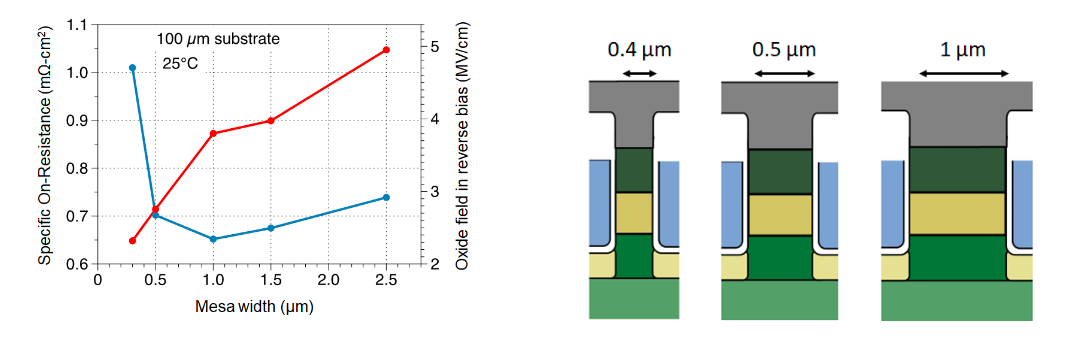
In the on-state
Reducing the mesa width increases 𝑅𝑜𝑛,𝑠𝑝, since the JFET region pinches off.
Increasing the mesa width above 1 µm also increases 𝑅𝑜𝑛,𝑠𝑝, since this increases cell area.
In the blocking state
The shield implant protects the oxide, but at mesa widths above 1.5 µm the oxide field exceeds 4 MV/cm.
Increasing mesa width increases the likelihood of base punch-through.
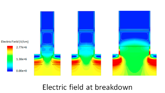
Mesa width is optimized for min 𝑹𝒐𝒏,𝒔𝒑 keeping the oxide field below 4 MV/cm
Fabrication process
Unit process development
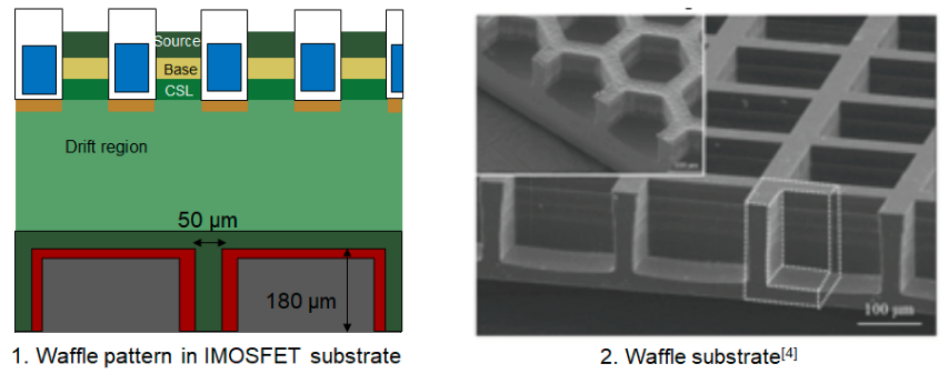
Waffle substrate
The 𝑅𝑜𝑛,𝑠𝑝 of SiC MOSFETs is limited by its substrate resistance. By decreasing the thickness of substrate, the resistance of the device can be reduced significantly. However, thinner substrate compromises the device strength. Waffle pattern can be used to remove material from the substrate, decreasing its resistance without compromising device’s strength.
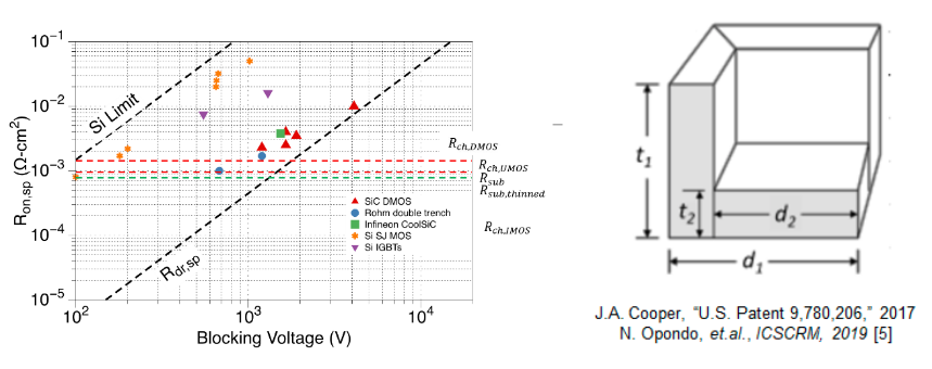
𝑅sub = ρt
Rwaffle= ρt2 (d1/d2 )^2
With 𝑡2=20 µ𝑚 and 𝑑2/𝑑1 =0.8,
𝑅waffle is 3.5X lower than 𝑅𝑠𝑢𝑏