|
PROBLEM:
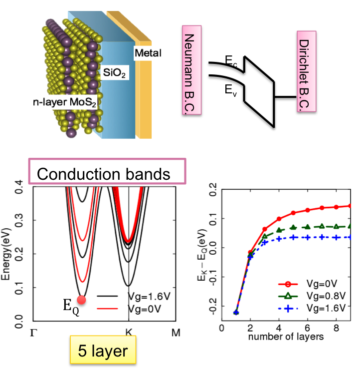
How does gate voltage affect the 2D material?
OBJECTIVE:
Study the band structure change under the gate voltage.
APPROACH:
- Schrodinger-Poisson solved.
- Wannier function basis is used for device Hamiltonian.
RESULT/IMPACT:
- DFT–equivalent, but efficient Hamiltonian used to accurately describe MoS2 devices
- Band offsets are function of gate voltages and layer thickness
- Valley wave functions differ significantly in their spatial distribution
- Different gate response of the 2 conduction band valleys. This can serve for switching device applications
|
|