
Preliminary Power Schematic
January 14, 2009 (1.0 hours):
Met with team to discuss a preliminary project proposal, a camera tracking system based on audio inputs. The basic idea was to keep a camera focused on a lecturer by tracking his voice. Alternative methods, including an ultrasonic source, were also considered. A project proposal sponsored by Southwest Research Institute was also discussed as an alternative.
January 14, 2009 (3.0 hours):
Met with team to discuss the project proposal sponsored by Southwest Research Institute in more detail. A preliminary project proposal was written. Southwest's main interest in the project was to implement the lossless Rice compression algorithm via a DSP or FPGA. An audio input would be converted using the algorithm to FLAC format. All team members expressed more interest in Southwest's project than the camera tracking project, mainly because the camera tracking system was poorly thought out.
January 15, 2009 (1.0 hours):
Met to discuss and finalize the preliminary project proposal. It was decided to build an audio recorder using lossless compression. An audio input, either analog or from a USB hard-drive, would be converted to FLAC format using the Rice algorithm. The FLAC files would then be saved on a USB hard-drive. The user interface was decided to be a touchscreen. It was also decided to look into using an FPGA with an embedded softcore rather than using an external micro-controller.
WEEK 01 SUMMARY
Accomplishments: Submitted preliminary project proposal.
Weekly Work Total: 5.0 hours
Project Work Total: 5.0 hours
January 18, 2009 (1.0 hours):
Met as a team to discuss individual preparation research.
January 18, 2009 (1.0 hours):
Researched softcore FPGA's, how to use USB with a softcore FPGA, and how to implement the Rice algorithm.
January 19, 2009 (0.5 hours):
Met as a team with Karl to discuss the project proposal. He suggested simplifying the project by removing the touchscreen and USB requirements. Instead of writing the compressed files to an external drive via USB, the files could be stored in SRAM and played via external speakers. He also recommended using a separate FPGA and micro-controller. The FPGA would be used to implement the encoding/decoding and compression algorithms, while the micro-controller would configure the FPGA and control the user interface. The micro-controller could also record statistics that would be displayed on an LCD display.
January 19, 2009 (1.5 hours):
Met with team to discuss Karl's suggestions. A rough draft of the project's block diagram was drawn, and initial PSSC's were written. A project name was also decided: Audio Recorder Using Lossless Compression. We also started researching some components, specifically A/D converters. It was determined that a sampling rate of 44.1kHz would be used with the 12-16bit output that Karl recommended.
January 20, 2009 (1.0 hours):
Met with Ken, Mike, and later Dr. Meyer to discuss the PSSC's. Mike agreed with all of Karl's suggestions. He also recommended adding a UART in order to read what is stored in the SRAM. Dr. Meyer suggested removing the ability to store the compressed files in order to calculate the latency from compressing and decompressing the audio.
January 20, 2009 (1.0 hours):
Met with team to discuss the PSSC's and prepare for tomorrow's presentation. It was decided to keep the SRAM, but also have the ability to bypass it in order to calculate latency.
January 21, 2009 (2.0 hours):
Met as a team to write the final project proposal. The FLAC Codec was also researched and discussed. It was discovered that the analog audio signal should be able to be encoded in one pass. This will make it easier to deal with when writing the VHDL code.
WEEK 02 SUMMARY
Accomplishments: Submitted final project proposal and decided on the five PSSC's.
Weekly Work Total: 8.0 hours
Project Work Total: 13.0 hours
January 26, 2009 (0.5 hours):
Met as a team to discuss the design constraints homework. It was decided to individually research all of the major parts. That way all team members could get a feel for what the design will require. Later in the week, the individual research will be shared and discussed.
January 27, 2009 (1.0 hours):
Started looking for parts. Today was focused on looking for A/D and D/A converters and SRAM. For A/D, I looked for 16bits at around 44.1kHz. I tried to match the D/A converters to the A/D, but wasn't sure about what parameters were needed. As for SRAM, I looked for 16MB, but really had no idea what I was looking for.
January 28, 2009 (1.5 hours):
Spent some time reading about FLAC (FLAC website), and then tried to pick an FPGA and micro-controller. I looked at Xilinx Spartan 3A FPGA's, but wasn't sure about the sizes needed. As for micro-controllers, I looked for an 8-bit controller with UART. I was able to find some made by Atmel. Microchip only had 16-bit controllers with UART.
January 29, 2009 (1.0 hours):
Met with Ken and Curt to discuss the parts that we researched. We decided that it would be in our best interest to talk to Mike and Karl about which parts we should choose. Several questions were written to ask them.
January 30, 2009 (1.0 hours):
Met with Ken, Curt, Mike, and Karl to discuss design constraints and chip selection. Mike and Karl recommended doing all of the major computations (linear predictive coding and compression) in the FPGA. We made some very rough estimates of the number of registers and RAM for the FPGA. It was also recommended to use a VCO and a clock buffer to drive the clocks for the various chips. Mike and Karl also suggested looking into getting a FIFO instead of SRAM because it would be easier to use.
January 31, 2009 (1.0 hours):
Did more research on FLAC. Specifically, I read more about linear predictive coding. ([PDF])
WEEK 03 SUMMARY
Accomplishments: Started researching parts.
Weekly Work Total: 6.0 hours
Project Work Total: 19.0 hours
February 1, 2009 (1.5 hours):
Met with Ken and Curt to select parts. We then decided to meet with the TAs again to discuss the parts we chose.
February 2, 2009 (1.0 hours):
Met as a team to look for a VCO and SRAM.
February 3, 2009 (1.0 hours):
Met as a team to prepare for tomorrow's presentation. We also decided that we would be using an Atmel Cyclone3 for the FPGA.
February 4, 2009 (3.0 hours):
Met as a team to work on the design constraint report. Based on feedback from today's presentation, we chose a 16bit ADC (ADS8506) and DAC (DAC7621). We also discovered that SRAM and FIFO are not made in the size needed for this project. We will ask the TAs about Flash or SDRAM tomorrow.
February 5, 2009 (5.5 hours):
Met as a team to work on the design constraint report. Because of how frequently data will need to be written to memory, we decided to use SDRAM. AJ got a Cyclone II development board earlier. We realized that we could use many of the same parts that are on the development board. This will allow us to do prototyping on the development board with reasonable expectations for our code to work with our design without modification. We also decided to replace the ADC and DAC with an Audio Codec (WM8731). This will reduce the cost and complexity of our design.
WEEK 04 SUMMARY
Accomplishments: All of the major parts for the project were selected. An Altera Cyclone II development board was obtained so that development of code can start.
Weekly Work Total: 12.0 hours
Project Work Total: 31.0 hours
February 8, 2009 (2.0 hours):
Met as team to start working on the Packaging Design homework. We found the sizes and package types for all of the major chips that we are using, and found two similar products to analyze and compare.
February 9, 2009 (1.0 hours):
Met as a team to continue work on the Packaging Design homework. More information about the similar products was found. Information about the Olympus LS-10 can be found here: LS-10.
February 10, 2009 (2.5 hours):
Met as a team to work on the Packaging Design report.
February 11, 2009 (3.0 hours):
Met as a team to continue work on the packaging report. We also looked for many of the "non-major" components that are necessary for the device to work, such as voltage regulators, connectors, jacks, and the RS-232 transceiver chip (MAX232).
February 13, 2009 (2.5 hours):
Started work on the schematic by looking for symbols for the major parts. These symbols were all added to the parts library in Orcad.
February 14, 2009 (5.0 hours):
Worked on the schematic. I finished finding/making schematic symbols for the major parts, and started "filling in" the circuit. I focused on the FPGA. The pin-out of the FPGA can be found here: [pdf]. I added the bypass capacitors for VCCA and VCCD_PLL, and configured the FPGA to be programmed by JTAG only. The circuit I drew is based off of Figure 10-25 (page 58) of Cyclone III Device Handbook Volume 1. Chapter 10. Configuring Cyclone III Devices. This configuration may have to change because I found out that the EEPROM for the FPGA is not directly programmed by JTAG (App Note 370). Instead, the FPGA acts as a bridge between the JTAG connector and the EEPROM. Figure 10-3 (page 12) of the Configuring Cyclone III Devices document may be useful for figuring out how to connect the EEPROM.
WEEK 05 SUMMARY
Accomplishments: As a group, we decided what the packaging constraints of the project should be, and also chose a better name for the project, "ALF". I started work on the schematic by finding symbols for the major parts, and drawing the power (for the FPGA) and JTAG parts of the circuit.
Weekly Work Total: 16.0 hours
Project Work Total: 47.0 hours
February 15, 2009 (5.0 hours):
Met as team to work on the schematic. I reconfigured the FPGA and EEPROM for AS configuration. I also drew the circuit to connect the SDRAM and Audio Codec to the FPGA.
February 16, 2009 (3.5 hours):
Met as team to work on the schematic.
February 17, 2009 (4.0 hours):
Met as team to work on the schematic.
February 18, 2009 (1.0 hours):
I added a JTAG connector to configure the microcontroller and added some signals to the debug header.
February 18, 2009 (3.5 hours):
Met as team to work on the schematic and report.
February 19, 2009 (2.5 hours):
Met with Curt and AJ to finish the schematic and report. We also started on the layout. There are three pages to the schematic (see below): Power, Config_PIC, and SDRAM_Audio. Power has all of the voltage regulators and bypass caps for the FPGA. Config_PIC has the configuration components for the FPGA and the microcontroller. SDRAM_Audio has the SDRAM and Audio codec.
|
Preliminary Power Schematic
|
 |
Preliminary Config_PIC Schematic
|
 |
Preliminary SDRAM_Audio Schematic
|
WEEK 06 SUMMARY
Accomplishments: As a team, we finished drawing the preliminary schematic and wrote the theory of operation report. I put most of my time into drawing the schematic. I made sure it was kept up to date, and made most of the necessary changes to it as the design changed.
Weekly Work Total: 19.5 hours
Project Work Total: 66.5 hours
February 22, 2009 (9.0 hours):
Worked on the PCB layout. I selected temporary footprints for all of the components. I then made a board outline and placed all of the components inside of the outline. I worked with AJ to reassign some FPGA pins in order to reduce the amount of traces going from one side of the board to the other side.
February 23, 2009 (5.0 hours):
I continued working on the layout. I moved some components around (mostly capacitors) to try to make routing easier. I routed the SDRAM chip.
February 24, 2009 (5.5 hours):
More work on the layout. I rerouted the SDRAM chip to try to equalize trace lengths.
February 25, 2009 (6.0 hours):
The SDRAM chip routing was still messy and uneven, so I worked with AJ to reassign the FPGA pins going to the SDRAM. I then rerouted the traces again. This time I think it looks good.
 |
SDRAM
|
February 26, 2009 (1.0 hours):
Started routing all of the capacitors for the FPGA. I tried to place each cap under its respective pin. The two "power islands" were placed in the middle.
 |
1.2V Bypass Caps
|
 |
3.3V Bypass Caps
|
 |
1.2V Power Island
|
 |
2.5V Power Island
|
February 26, 2009 (5.5 hours):
Continued working on the capacitors. I also started thinking about how the ground planes would work for this board. There are four voltages: 5.0V, 3.3V, 2.5V, and 1.2V. The 3.3V will be the biggest plane because most of the components use this voltage level.
February 27, 2009 (5.0 hours):
I finished routing the FPGA power and ground pins. I also routed traces to most of the other components. The Audio Codec and its supporting components are the only parts left to route.
WEEK 07 SUMMARY
Accomplishments: As a team, we completed the PCB layout narrative report and made a preliminary PCB layout. All of my time was spent working on the preliminary layout. I routed traces to most of the components and updated the schematic as necessary.
Weekly Work Total: 37.0 hours
Project Work Total: 103.5 hours
March 1, 2009 (4.5 hours):
Completely finished routing the PCB. There are still some things left to do, but the majority of the work should now be done. A few footprints need to be changed, power and ground planes need to be added, and some trace widths need to be modified. There will be four power planes: 5.0V at the top of the board, 2.5V underneath it, 1.2V under the FPGA, and 3.3V everywhere else. The ground planes will match the power planes with an added analog ground in the bottom right corner. See concept picture below.
 |
Preliminary Layout
|
 |
Power Plane Concept
|
 |
Ground Plane Concept
|
March 1, 2009 (2.0 hours):
Performed a design rules check on the layout and fixed all of the errors (started with over 2000). Most of the errors were just spacing issues that were easily resolved.
March 2, 2009 (3.0 hours):
Met as a team to prepare for Wednesday's design review. We figured out which parts each team member will be presenting. I will present most of the PCB layout (focusing on the FPGA and power) and the timeline for finishing the project.
March 3, 2009 (6.0 hours):
Met as a team to finished the design review presentation and printed out the handouts necessary for the design review. After Curt and Ken left, I practiced a little with AJ in order to figure out what I was going to say.
March 6, 2009 (4.0 hours):
Today was the first meeting after the design review. After considering the feedback from the review, we decided to replace the VCO and JTAG. Instead we will be using a 100MHz oscillator to clock the FPGA and ICD2 to program the microcontroller. We also reworked the the reset and audio CODEC circuitry. We will now be using line-in instead of mic-in and stereo instead of mono.
March 7, 2009 (7.0 hours):
After making changes to the schematic, I realized that major changes would have to be made to the PCB layout. I discussed it with the rest of the team and decided to completely reroute the board. This time I started with the FPGA capacitors. I rearranged them with the power planes in mind, and spent the rest of the night routing them.
 |
1.2V Bypass Caps
|
 |
3.3V Bypass Caps
|
 |
Power Islands
|
WEEK 08 SUMMARY
Accomplishments: As a team, we gave our design review and incorporated some of the suggestions into our design. I updated the schematic and started rerouting the board.
Weekly Work Total: 26.5 hours
Project Work Total: 130.0 hours
March 8, 2009 (6.0 hours):
I spent today continuing work on the PCB layout. I finished routing the FPGA capacitors, and then routed the rest of the power and ground traces. While routing the different power and grounds, I kept in mind the shape of the power and ground planes. After that, I routed the SDRAM traces.
March 9, 2009 (5.0 hours):
Today I finished routing the PCB. I also added all of the power and ground planes. See the pictures below.
 |
Final Layout
|
 |
Top Layer
|
 |
Bottom Layer
|
 |
Power Plane
|
 |
Ground Plane
|
March 13, 2009 (1.0 hours):
AJ gave me a call this morning saying that the FPGA pitch was wrong. It took us a while to figure out that distance between the pins is not the same as the pitch of the pins. In the end, no changes needed to be made.
WEEK 09 SUMMARY
Accomplishments: Finished and submitted the PCB layout.
Weekly Work Total: 12.0 hours
Project Work Total: 142.0 hours
WEEK 10 SUMMARY
Accomplishments: Spring Break...a much needed break.
Weekly Work Total: 0.0 hours
Project Work Total: 142.0 hours
March 23, 2009 (2.0 hours):
I found some sample code for the PIC microcontroller. I found examples for a SPI Master and UART. Example Code Folder
March 24, 2009 (4.0 hours):
We got our PCB today. I took some time to ohm out the board. I checked all of the power and ground connections and vias. I didn't find any problems.
March 25, 2009 (5.0 hours):
Today I soldered on the 5.0V and 1.2V regulators and supporting components. It took a very long time for me to find a decent tip for the soldering iron. Most of the tips are in pretty bad shape. There was a minor problem with the power jack. The schematic had an error which resulted in the wrong pin being connected to our power switch. Since the switch will be mounted off of the board with wires connecting to the PCB, an easy fix was made: one of the wires was soldered directly to the power jack pin instead of the intended via. The fix worked and the regulators seem to be working fine. After realizing that we don't have the 3.3V/2.5V regulator, we quickly ordered it. Hopefully it will be here on Friday. More testing of the regulators will take place once they are all on the board.
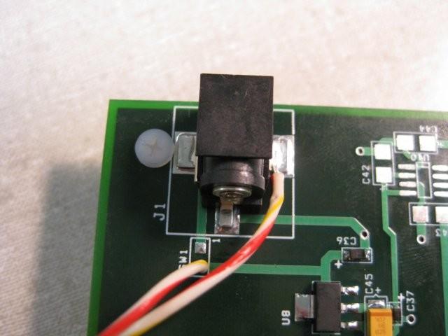 |
Flywire 01
|
March 26, 2009 (0.5 hours):
I looked over AJ's software report. It looked good for the most part; there were just some minor grammatical errors.
March 27, 2009 (0.5 hours):
I decided to buy a soldering station for myself today. Now I shouldn't have to waste a lot of time trying to find decent soldering tips.
WEEK 11 SUMMARY
Accomplishments: As a group we completed the Software Design Narrative, and spent a lot of time developing code. Most of the code is still in the initial stages of development. I helped find some example code and started populating our PCB.
Weekly Work Total: 12.0 hours
Project Work Total: 154.0 hours
March 30, 2009 (1.0 hours):
I started searching for some patents on which our project may infringe. Patent 7430328 looks very similar to ALF. Several other patents are for lossless compression/decompression, but I think there are enough differences that they won't cause any issues. The patents I found are linked in this Patent Portfolio.
April 1, 2009 (4.5 hours):
I got my soldering station yesterday, and put it to use today. I started with the 0402 capacitors.
 |
0402 Capacitors
|
April 2, 2009 (4.0 hours):
Today I continued soldering 0402 packages. These are very small components and take a lot of time to solder correctly. I only have about 10 left.
April 3, 2009 (3.5 hours):
Today I finished soldering all of the 0402 packages. I also soldered on the FPGA.
 |
FPGA
|
April 4, 2009 (5.5 hours):
Today I soldered on the FPGA support components (oscillator and config). AJ then programmed the FPGA with a heartbeat program. There were no problems. After that I soldered on the microcontroller and its support components. AJ programmed a heartbeat program into the microcontroller, and it also worked without any problems. Finally, I soldered on the LCD header and level shifter so that AJ could try to get it working after I left the lab.
 |
FPGA and microcontroller with LCD
|
 |
Bottom of board
|
WEEK 12 SUMMARY
Accomplishments: As a group a lot of time was spent developing code. The LCD is working, but the rest of the code is still in the early stages. I spent all of my time populating the PCB. There are only a few components left to put on the board (Audio CODEC, SDRAM, and debug).
Weekly Work Total: 18.5 hours
Project Work Total: 172.5 hours
April 5, 2009 (3.0 hours):
Today I finished populating the board.
 |
Top of board
|
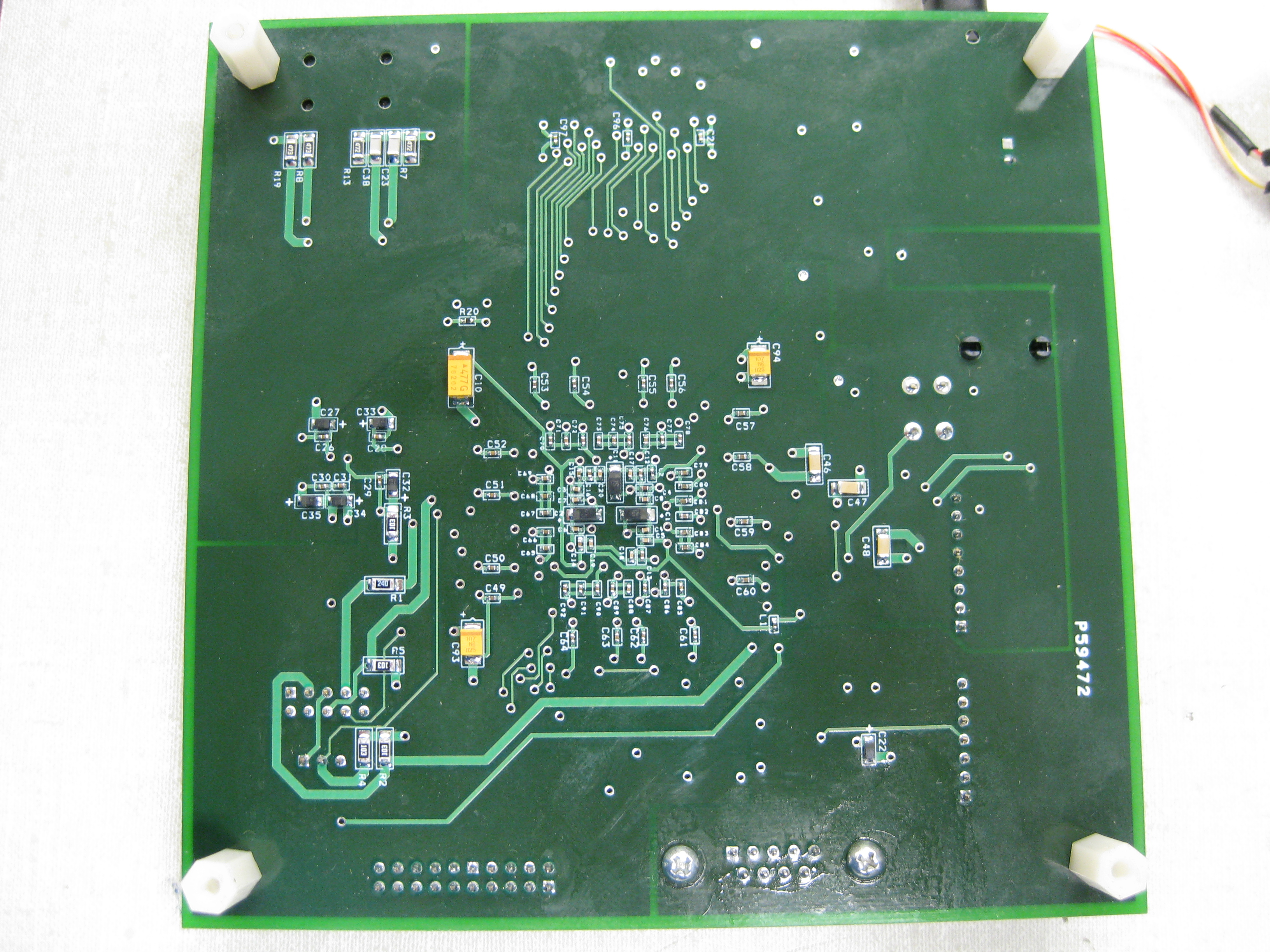 |
Bottom of board
|
April 6, 2009 (1.0 hours):
I started working on the Reliability and Safety Analysis report that is due this week.
April 7, 2009 (4.0 hours):
With the help of Curt and AJ, I prepared for my Reliability and Safety Analysis presentation tomorrow. We decided on the failure criticality levels we would use, and tried figure out all of the possible ways our project could fail (regulators burning out, stuck-at faults, LCD not working, etc.). See this presentation for more detail: Reliability and Safety Analysis Presentation.
April 8, 2009 (2.0 hours):
Worked on the report some more. I finished writing the safety part. Based on suggestions from my presentation, I changed the "medium" criticality failures for the regulators to "high" criticality failures.
April 9, 2009 (5.0 hours):
I finished writing and submitted the Reliability and Safety Analysis report.
April 10, 2009 (4.0 hours):
Today I worked with Curt on trying to get the Audio CODEC working. We tried to see the signals on all of the pins of the CODEC, but mostly just saw noise. We then did the same thing with the dev board, but got the same results. This means that the results we got are meaningless because the dev board audio works but ours doesn't.
April 11, 2009 (5.0 hours):
Met as a team to continue work on coding. I helped AJ and Curt with debugging the Audio CODEC. We finally realized that the problem was with the acknowledge signal being sent by the CODEC. After we commented out the line of code with the error, the CODEC worked. I then helped Ken figure out what menus and information should be displayed on the LCD. We decided that one pushbutton would be used to cycle through the menus while a second button would make selections as needed. The other two buttons were decided to be unnecessary. After dinner, I helped AJ and Curt with getting the SDRAM working. Right now we are having problems getting the Nios processor to work on our board. We are looking into other options.
WEEK 13 SUMMARY
Accomplishments: As a group, we got the Audio CODEC working and continued to debug the rest of our code. Right now we are focusing on the SDRAM. I finished populating the PCB, wrote the Reliability and Safety Analysis report, and helped debug code.
Weekly Work Total: 24.0 hours
Project Work Total: 196.5 hours
April 12, 2009 (4.0 hours):
The reason why we can't use the Nios processor with our board is because it has to be programmed using JTAG. We don't have a JTAG connector on our board. Curt and I looked into adding one, but we realized that we would have to first remove the FPGA in order to cut traces that are underneath it. I then worked with AJ and Curt on the SDRAM. I found some source code that we are editing to meet our needs. I left before the we were ready to test it.
April 13, 2009 (4.0 hours):
I looked for (and found) source code for an SPI slave and a UART controller: SPI slave, uart. These should both work with very few modifications needed. I then made some cables to go from the LCD and FPGA debug headers to a breadboard. These cables will make future debugging more convenient.
April 14, 2009 (4.0 hours):
Today I worked with AJ on getting the SDRAM to work. We were able to successfully test it. Then we worked on getting both the Audio CODEC and SDRAM code to work at the same time. After fixing a few bugs, it was working.
April 15, 2009 (4.0 hours):
I started looking at the SPI code to figure out what modifications I would have to make. I think all I have to do is make two registers: one to store data received from the microcontroller and one to store the data that will be sent to the microcontroller. I then helped AJ try to figure out what is wrong with our Audio CODEC code. We think it is bypass mode, and we can't figure out why.
April 17, 2009 (4.5 hours):
Worked on the SPI code for the FPGA. This is the source code I am now using: (SPI website). I first set up the dev board switches and keys to act at the master (with me manually clocking the SCLK), and used the LEDs to see the registers. This helped me figure out exactly how the code was working. Then, working with Ken, I connected the microcontroller dev board to the FPGA dev board in order to test the code with the microcontroller as the master. It didn't work, but I realized after I left that we didn't connect the boards correctly.
April 18, 2009 (6.5 hours):
Ken and I were able to successfully test the SPI on the dev boards. We are now trying to get it to work on our board. Ken is having problems getting the SSEL pin to work properly on the microcontroller. While he was working on that, I started working on the UART code. The main problem with the UART is going to be figuring out how to clock it correctly. I decided to use this (uart) as my source code because it includes a baud generator and explanations of how the code works. I'm still trying to figure out the clock though. The FPGA has a 100MHz clock and we are planning on using the UART at 9600 baud. The baud generator generates a ticks at 16*(baud rate), so it needs to generate a tick every 651 clock cycles (100/(9600*16)). I think all we need is a counter to do this, but for some reason the baud generator is more complicated.
WEEK 14 SUMMARY
Accomplishments: As a team, we continued the development of the software for out project. The SDRAM and Audio CODEC are both working, but separately. The next step is to take data from the Audio CODEC and store it in the SDRAM before playing it. I worked on the SPI and UART code. The SPI is the communication bus between the FPGA and microcontroller. The UART will be used to dump data from the SDRAM to a computer for debugging.
Weekly Work Total: 27.0 hours
Project Work Total: 223.5 hours
April 20, 2009 (4.0 hours):
Worked a little more on the UART code. It partially works. I'm able to send something to the computer and see it in Tera Term Pro, but its nonsense data. I may come back to this later, but UART really isn't very important for the project so I'll spend my time working on higher priority things. I then worked with Ken on the SPI code. For some reason it works on the dev board, but not our board. Ken was having problems with SSEL, so we added a flywire from a microcontroller gpio to an FPGA gpio. We added a second flywire in order to have an asynchronous reset for the FPGA.
April 21, 2009 (4.5 hours):
Today I met with Ken to get the SPI code working on our board. The problem ended up being in the FPGA code. Earlier, we added a state machine that interprets the messages sent by the microcontroller. The problem was that a signal was never going high and the FPGA thought it was receiving invalid data. We removed that check (it wasn't really needed anyway) and the SPI worked. I then started working on the User Manual that is due this week.
April 22, 2009 (2.0 hours):
Today I worked some more on the User Manual.
April 23, 2009 (6.0 hours):
We got our box (for packaging) today. Curt, Ken, and I machined the holes necessary for the LCD, pushbuttons, and jacks. I then put it all together. We still need to add labels for the power switch, pushbuttons, and jacks.
 |
Packaging
|
WEEK 15 SUMMARY
Accomplishments: As a team, we rewrote three of our PSSCs because FLAC is not achievable in the remaining time. We also wrote the User Manual and packaged our design. I worked with Ken to get the SPI working.
Weekly Work Total: 16.5 hours
Project Work Total: 240.0 hours
April 26, 2009 (3.5 hours):
Started gathering things together to write the final report. Also started to edit some of the previous reports that will be included in the final report.
April 27, 2009 (2.0 hours):
Edited some more of the previous reports and the block diagram.
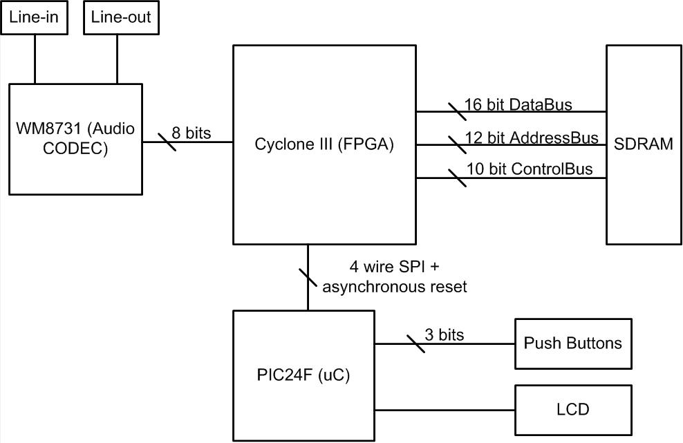 |
Block Diagram
|
April 28, 2009 (4.5 hours):
Met as a team to make the video for the bonus presentation. It shows all five of our PSSC working.
April 29, 2009 (4.0 hours):
Worked more on the final reports, and put together a presentation for Friday.
April 30, 2009 (2.0 hours):
Worked more on the final reports.
May 2, 2009 (7.0 hours):
Finished the final reports. Below is a picture of us with the final product.
 |
Group Picture
|
WEEK 16 SUMMARY
Accomplishments: We finished ALF and wrote various final reports. We also made our demonstration video. I updated the block diagram and worked on the reports.
Weekly Work Total: 23.0 hours
Project Work Total: 263.0 hours