Bryan Hermsen's Lab Notebook
Week 01
August 22, 2007 (3 hour):
We met as a team after class and researched our origianl project idea to
determine if it is feasible or not. After researching different strategies, we determined that within the scope of the course we can not perform
signal processing that is sophisticated enough to determine what notes our guitar is playing.
August 23, 2007 (5 hours):
We discussed ways to complete the Guitar Ace project without relying on signal processing. We
discussed running circuit through the strings and fretts of the guitar and analyzing the guitar as a circuit, which would change according to which
srtings are pushed. This seemed promising for awhile, but when three or more strings are pushed simultaneously to adjacent fretts, the same exact
circuit can be created by a variety of different note/chord combinations.
We then came up with three backup ideas to submit for our first proposal (due tomorrow):
1. Change Guitar Hero to Piano Hero and complete similar functions with a MIDI keyboard.
2. Make cell phone software that can control a home appliance such as an oven or microwave using a cell phone.
3. Make an interactive poker table that would determine which player is statistically more likely to win a given hand
and would possibly even track chip counts or bet and pot values.
WEEK 01 SUMMARY
Accomplishments: Determined our original idea was not feasible, and submitted preliminary project proposal.
Weekly Work Total: 8 hours
Project Work Total: 8 hours
Week 02
August 28, 2007 (4 hours):
Met as a team. We reviewed feedback from our PSSC proposal and made a made a final decision
concerning which project to pursue. Based on input from Professor Meyer, we decided to do the MIDI keyboard project idea. We also developed our PSSC's
for presentation in lab tomorrow.
August 30, 2007 (4 hours):
Met as a team to adjust our PSSC's per feeback in lab. Made some decisions about the project.
- We wanted our display to appear similar to Guitar Hero, in the sense that a
bar (of length corresponding to length the note should be pressed) scrolls down
the display above the appropriate key and the user presses the key until the
bar is finished scrolling.
- The game would be stand alone, and have capability of loading new MIDI
keyboard tracks via USB and generating the bar display on the fly.
- We will output the sound as long as the user is playing it correctly,
otherwise a negative sound will play.
- A running tally of your score will be displayed, as well as how many
consecutive notes you have played without error.
- If time allows, we will add a composing feature that allows you to record
your own MIDI tracks.
To see more details...Here is our
Final Project Proposal (HW2)
WEEK 02 SUMMARY
Accomplishments: PSSC and project proposal finalized.
Weekly Work Total: 8 hours
Project Work Total: 16 hours
Week 03
September 4, 2007 (1 hour):
Met as a team to discuss Design Criteria. We discussed and researched VGA interface options,
and we discussed memory contraints. A working draft of our requirement considerations is available at
H:\public-web\Notebooks\Notes\Micro-Requirements.doc
September 5, 2007 (1.5 hour):
Worked independently, researching VGA display. See
H:\public-web\Notebooks\Notes\VGA_Research.doc
September 9, 2007 (1.25 hour):
Met as a team to discuss what needs to be done this week. We came up with the following assignements:
Curtis - Eval Board and Micro/FPGA (canidates by Monday, sample by Tuesday)
Tom - Monitors and Software Block Diagram (Friday)
Vik - Power Supply Design (voltages needed) and help find micro (Tuesday)
Bryan - Block Diagram and initial parts list (Thursday Night), HW3 by Friday at noon
WEEK 03 SUMMARY
Accomplishments: Discussed Design Criteria and
micro-processor constraints.
Weekly Work Total: 3.75 hours
Project Work Total: 19.75
Week 04
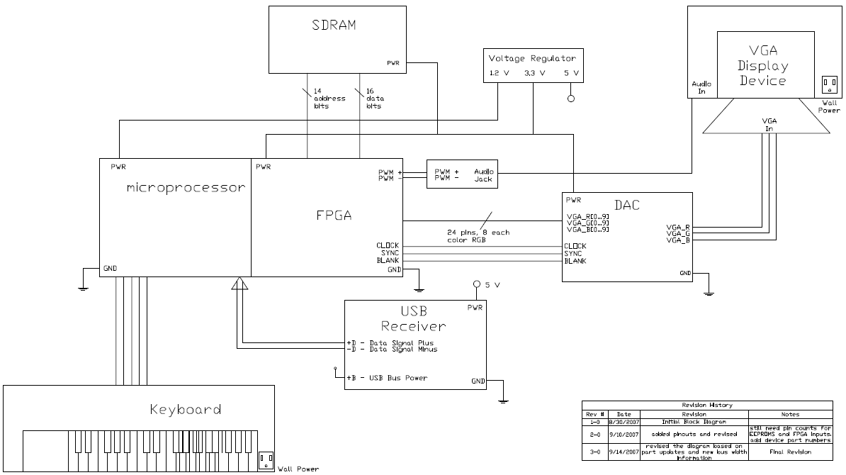
September 10, 2007 (3 hours):
Worked individually on block diagram.
Made the following updates and created Block_Diagram_v2-0.pdf:
- USB pins based on pinout found online. (ELEXOL-USBMOD5[1])
- DAC and FPGA pins based on Altera schematics. (DE2_scheamtics)
September 11, 2007 (1 hour):
Created presentation for class.
September 13, 2007 (1 hr):
Worked on HW3 document individually.
Question: will audio be part of performance feedback?
September 13, 2007 (1 hr): Met as a team to discuss several parts. Phil and Karl recommended we use SDRAM instead
of EEPROM to store extra MIDI. We found specific part numbers for some of the parts we're using. I created Revision 3 of the block diagram
to show the proc and the FPGA as one chip. We chose Atmel's EP2C20 FPGA for because it had the largest number of logic components for the
non-BGA devices.
September 13, 2007 (1 hr): Worked on HW3 and Block Diagram.
Curtis and I decided that audio WILL be part of performance feedback. We will not play the MIDI when the user misses a note. There may be some sound
added to indicate that they are incorrect, too.
September 13, 2007 (7.5 hr): Worked on HW3 document.
Questions:
-Tom: Computation section (2.1) Anything missing?
-->Nope
-Tom: How much memory do we need...
-->
-Curtis: Clock Speed calculation?
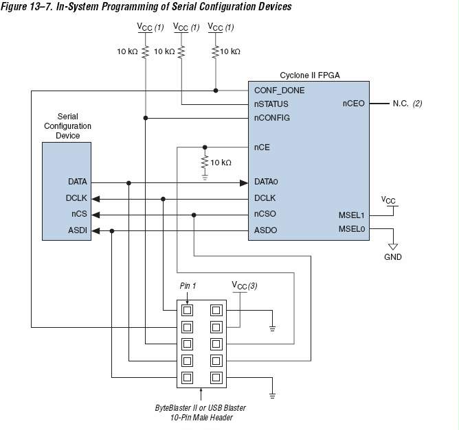
Researched some parts. Today we chose to use the EP2C20 FPGA. I noticed that this part is compatible with several Configuration Devices. Not
knowing what a Configuration Device really is, I looked it up and found this document: Altera
Configuration Documents A configuration device contains the configuration data for the FPGA. During operation, the FPGA stores its configuration
data in SRAM, which is volatile and does not stay through a power-cycle. When the device powers up, the FPGA needs to get its configuration data
from a configuration device. So... we're going to need one of these.
I also addressed the memory constraints of our project. To start doing this I did more research on the Cyclone II architecture and the memory
available on it. That led me to this document: Cyclone II Memory Blocks. From that document I
learned that the Cyclone II has M4K memory blocks which each have 4,096 memory bits. (p.1) The EP2C20 has 52 of these blocks for a total of 239,616
bits (p.2).
Furthermore, the Cyclone II has built in support for external memory devices, including SDRAM. I found this document about External Memory Interfaces. On Page 1 it notes that "Dedicated clock delay control circuitry
allows Cyclone II devices to interface with an external memory device at clock speeds up to 167 MHz/333 Mbps for DDR and DDR2 SDRAM devices."
Altera makes their own DDR and DDR2 SDRAM devices, but according to page 11, they are huge. The EP2C20 ones start at 240 pins.
I researched MIDI transmission specifications and found from home.concepts
that MIDID serial protocol uses a 31.25kHz baudrate (bps), no parity bit, 1 stop bit, and 8 data bits. The current through each pin is approximately 5ma.
That information was confirmed on page 10 of this document at rutgers.edu
From reading this page on usb2.net, it appears as though one MIDI pin sinks 5 mA and another
pin sources 5mA. On page 18 of this document at smsc.com, I found that the typical current
for a flash drive is 60-70 mA when active for a 3.3V supply, and <=150 microamps in standby mode. I assume that this current is sourced by the USB
since there is a power source in the USB pinout. Thus the microprocessor will sink 60-70 mA.
I found here that the Cyclone II
is compliant with 66-MHz operating frequency.
What still needs to be done:
- update block diagram to final form (SDRAM busses)
- Interface requirements: current sink/source vals
-
September 14, 2007 (2 hr): Met as a team (minus Vik) to discuss current draw of system components and to prooread
HW3.
Price for 5 V regulator
from Vik: Price for 1.2 V regulator
Price for DC Power Jack
WEEK 04 SUMMARY
Accomplishments: updated parts list and block diagram. defined design constraints for HW3
Weekly Work Total: 16.5
Project Work Total: 36.25
Week 05
September 17, 2007 (2 hrs.): Met with Curtis and Tom:
Things we decided:
Input to microprocessor software:
1. MIDI Input from keypbard (through optical isolator)
2. Stored MIDI data from flash
Output from micro to FPGA
1. Note and duration from MIDI for note bars
2. Tempo from MIDI and from potentiometer
3. Note played on keyboard
4. Score, song title, general game info
Hardware input
1. All outputs from micro listed above.
2. Stored images (title, song selection, keyboard database)
Things we need to do soon:
*Preliminary Schematic by Friday (due for HW5 next week)
- look at part circuit diagrams and see how each part interacts with a larger circuit.
- determine what other components are needed (i.e. resistors, caps, optical-isolators)
*Packaging Design by Friday (due for HW4)
Additions to parts list:
1. optical isolator for MIDI input
2. MIDI jack for PCB board
September 18, 2007 (3.5 hrs.): Met as a team to discuss packaging and schematic.
Schematic Considerations
- The DE2 development board uses a "USB Blaster"
I worked on schematic, created parts.
September 19, 2007 (1.5 hr.): Worked on parts more. Curtis showed us some cool MIDI
decoding information and we started figuring out how a MIDI file is interpreted by a synthesizer.
September 20, 2007 (1.5 hr): Found DAC and added it to parts list. Started working on
dimensioned AutoCad drawing of preliminary PCB. Then I started reading info on fpga4fun.com
Links:
-Parts List
-Initial PCB drawing
-FPGA4Fun.com
September 23, 2007 (15 min.): Talked to Tom about project status and what we should do tomorrow:
1. MIDI: we are probably ready to get the keyboard and start trying to accept MIDI input.
2. software: waiting on Tom's meeting with Mark Johnson
3. discuss HW 5
4. order parts that need ordering
WEEK 05 SUMMARY
Accomplishments: Developed a better understanding of the physical design of the project, including the parts that we need, how the circuit
will be laid out, and, at a preliminary level, what the PCB will look like. Also got a better understanding of the DE2 board that we are using.
Weekly Work Total: 8.75
Project Work Total: 45
Week 06
September 24, 2007 (2.75 hr): Met as a team:
I ordered 2 samples of the DAC from Rathsburg Associates. They should be here by the end of next week.
I left a message with NXP Semiconductors (919-677-7997) regarding the USB controller (Philips ISP1362)
I went through and made sure that every part on our preliminary PCB layout is included in the parts list, and made note of parts that still
need to be added to both the parts list and the PCB drawing:
- MIDI jack
- USB port
- small components (resistors, caps, etc.)
- optical isolator
I started looking through the data sheet for the DAC to analyze its pinout.
--> DAC-related questions:
- - -> will the micro control the !BLANK signal?
- - -> can we tie !SYNC to ground?
- - -> Vaa: do we want 3.3V or 5V? (see below)
- - -> CLOCK: I assume that's from the FPGA, right?
- - -> !IO(R/G/B): do we need these complementary outputs or should we tie them to ground (per data sheet p. 7)
--> DAC-related discoveries:
- - -> Our 330Hz version is only available in the 3.3V variety. Thus Vaa=3.3V
- - -> We need 3, maybe 6 75ohm resistors for IOR/B/G, (maybe for !IOR/B/G)
[see note 9/25]
- - -> We need a .1 micro-farad ceramic cap for the COMP pin.
September 25, 2007 (1.25 hr):
Discussed with Tom and Curtis:
- VGA output from DAC:
- -> we don't need !IOR/G/B: those are for differential inputs that eliminate noise by subtracting
- -> the 75 ohm resistors mentioned yesterday are not as i thought. Instead, it means that the outputs are capable of being delivered over a
75 ohm coaxial cable. So our cable had better not have a higher resistance than that. Does this mean we should use coax?
- -> VGA info that Tom has said that the output of the DAC should go through a 1kohm resistor, and the resistor should lead to the VGA connector but
has a bypass diode to ground. So we actually need 3 1k resistors.
- The DE2 development software isn't working: we should meet with Mark Johnson to see if he knows how to use it.
Individual work:
- ORCAD symbols: all symbols we use will be added to our library (477grp2:\Analog Devices Lib]\GROUP2CUSTOMLIB)
- continued looking at DAC pinout. Still about 6 pins to look at.
September 26, 2007 (1 hr): Met as a team
Discussed SRAM usage with Tom. 2 options:
1. Use a 24-bit data bus SRAM. Send all RGB intensity data for one pixel from FPGA to SRAM on each write cycle, and read all RGB intensity data
for one pixel on each read cycle with DAC.
2. Map the colors and choose how many we need. For 256 colors, use an 8-bit data bus to read and write to the SRAM. Data read from the SRAM goes
back to the FPGA where it is decoded, and then a 24-bit data bus goes from the FPGA to the DAC
** In each case, timing characteristics need to be carefully considered.
I looked at dual-port 1M x 8 SRAM chips on mouser but they are all obsolete or BGA.
September 26, 2007 (4 hr) : Worked individually.
More from the DAC data sheet:
-> CLOCK calculations:
Dot Rate = (Horiz Res) x (Vert Res) x (Refresh Rate)/(Retrace Factor)
Dot Rate = 640 x 480 x 60/0.8 = 23040000 = 23.040MHz
- Note:
Refresh Rate = frequency at which screen is refreshed. (60 times per second)
Retrace factor: accounts for the time that the time that the display is blank while incrementing to the next row.
Rset value determines the amplitude of the output video level
September 27, 2007 (0 hr):It's about time I put this up here:
Block Diagram
Created for Homework 3
September 27, 2007 (11 hr): Worked individually. Read more of the DAC datasheet
and created the DAC schematic.
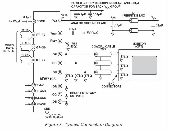
Some important PCB layout notes from the DAC datasheet from page 11-12:
- Good decoupling is important.
- lead length between groups of Vaa and GND pins should be minimized.
- PCB board should have two distinct power planes: analog and digital
- All ground should come to a single point in a ferrite bead.
- All Vaa power should come from a single point that connects to the PCB power (Vcc) in a single ferrite bead. This bead should be within three inches of the ADV7125.
- Noise on the analog power plane can be further reduced by decoupling, optimuly achieved with .1 microF ceramic capacitors. Each of the two Vaa groups should be individually decoupled to ground.
- The DAC should be as close as possible to the output connectors.
- Here's a Typical Connection Diagram:
VGA connector notes:
* Found pinout from Fall 2004: Schematic
Tom found the Cyclone II device pinout!
we finished the schematic in all its glory.
WEEK 06 SUMMARY
Accomplishments: Researched parts and created schematic. Did this by first ctreated symbols for OrCad, then creating circuit
local to each chip, including capacitors and resistors as specified by manufacturers. Finally combined all parts into a cohesive schematic.
Weekly Work Total: 20 hrs
Project Work Total: 65 hrs
Week 07
October 1, 2007 (2 hr): Met as a team:
- began putting Orcad Schematic into format for OrCad Layout. discussed work for week and parts ordering status.
October 2, 2007 (1 hr): Worked individually:
Programming the Cyclone II
- remember that the Cyclone II needs to get its configuration list from the flash
- Cyclone II Configuration Scheme Overview
- for prototyping purposes, Altera sells three types of
Altera Programming Cables
- one of these three, the ByteBlaster II Download Cables, is a standard parallel printer port for PC interface
- - a datasheet for the ByteBlasterII is saved on our drive here.
- - - Notes from ByteBlaster datasheet: (page #'s in ()'s)
- - - - requires 1.5-5.0 V from the target circuit board (6)
- - - - can be used in 1.8, 2.5, 3.3, 5.0 V systems. isn't ours 1.2??? But it says Cyclone II is supported
here.
- - - - pullup resistors are needed (6)
- - - - Quartus II software version 4.0 or later to configure device. Nios II IDE also supported
- - - - 10-pin header on device board
- - The next question is how do the Flash and the ByteBlaster interface with the Cyclone II. See section 13 of the Cyclone II Device Handbook,
Configuration. Page 20 has a
schematic
October 2, 2007 (9 hr):
Met as a team in the morning:
- Strategic Planning for the week. Came up with schedule, This Week.doc
- Discussed circuit schematic in preparation for meeting with Dr. Meyer this afternoon.
Met with Professor Meyer and Chuck in early afternoon:
- Decided to use a 4-layer PCB based on several factors:
- - pwr & gnd pins are scattered around the Cyclone II FPGA, intermittent with I/O pins
- - several different chips are interfacing with the FPGA (Flash, SRAM, DAC, MIDI synth)
- - 4-layer board is $66 (vs. $33 for 2-layer)
- - Careful consideration needs to be taken in order to isolate digital and analog ground planes.
After meeting with Dr. Meyer we met as a team:
- revised parts of the schematic
- looked more carefully at the Configuration Cables (see above, from last entry):
- - USB/ByteBlaster cables have circuitry in the cables. They are $300/$150 cables.
Can we sample?
I went throught the Layout Tutorial in OrCad and struggled with the program.
I created the PCB Layout Considerations presentation
October 3, 2007 (1.5 hr):
The source of our problems with Layout was pin inconsistencies. These were identified by running a Design Rules Check in Capture.
I fixed most of them, but three remain.
October 3, 2007 (6 hr):
Worked on report. The rest of the errors are out of circuit (thanks to my teammates)
Concerning Bypass Capacitors to FPGA Ground: Vik found this page
- Bypass and decoupling techniques are important for reliable operation, and become more important for increasing supply current.
- small caps with low series inductance are good for high-freq transitions. large caps continue to supply current after the high-freq caps are depleted.
- High-density packages such as ball grid array (BGA) may make it difficult to use one decoupling cap per Vccio and ground pin pair. In such cases, designers make every effort to use as many decoupling caps as allowed by the layout.
- Decoupling caps should have a good frequency response, such as monolithic-ceramic capacitors.
- Formula for total capacitance: --> equivalent switched logic array capacitance = (logic array power) / (VCCINT2 � clock frequency)
- We decided to ask Dr. Meyer tomorrow about the caps, and in the meantime we're adding caps so that there are 1 small one per vcc pin (33), 2 100microF near the chip, one 1.2V the other 3.3V, and 1 1000microF somewhere on the board between the voltage regulator and 100microF for each voltage.
I looked up capacitors on mouser.
EMI Considerations (from
Motorola App Note AN1259).
- Within a microcontroller system, the digital clock circuitry is usually the biggest geneartor of wide-band noise. [2]
The schematic is done! And so are the footprints! A switch was added, some capacitors were rearranged, headers and test points were finalized, the DRC was run and passed, the netlist was created, footprints were assigned to parts, and at long last we have... a rats nest.
October 4, 2007 (18 hrs):
Well, now seems as good a time as any to start routing.
We re-assigned a bunch of the FPGA pin assignments so that they are easier to route based on where the pins are on the various chips. Did lots of routing.
WEEK 07 SUMMARY
Accomplishments: Refurbished schematic for use with Orcad Layout, corrected errors and exported netlist. Arranged parts on the
PCB and editted pin assignments to facilitate routing. Routed PCB.
Weekly Work Total: 37.5 hrs
Project Work Total: 102.5 hrs
Week 08
October 10, 2007 (2.25 hr): Met as a team:
- worked on PCB touchup
- discussed PCB progress with course administrators
- divided up tasks for presentation
October 11, 2007 (2 hrs): Worked individually researching parts.
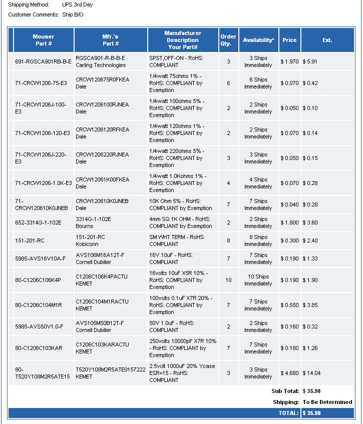
October 12, 2007 (4 hrs): Worked individually researching parts:
Resistors - Vishay/Dale Resistor Datasheet
75ohm: Vishay/Dale - CRCW120675R0FKEA - Mouser Search.
Need 3, ordering 6.
100ohm: Vishay/Dale - CRCW1206100RJNEA -
Mouser Search. Need 1, ordering 2.
120ohm: Vishay/Dale - CRCW1206120RFKEA -
Mouser Search.
Need 1, ordering 2.
220ohm: Vishay/Dale - CRCW1206220RJNEA -
Mouser Search.
Need 1, ordering 3.
1kohm: Vishay/Dale - CRCW12061K00FKEA -
Mouser Search.
Need 2, ordering 4.
10kohm: Vishay/Dale - CRCW120610K0JNEB -
Mouser Search.
Need 4, ordering 7.
1kohm potentiometer: Bournes - 3314G-1-102E -
Mouser Search.
Need 1, ordering 2.
Test Points: Kobiconn - 151-201-RC -
Datasheet -
Mouser Search. Need 5, ordering 8.
Switch Buttons:
Option 1: NKK - UB15...03.... - None ordered. (~$5 per)
Option 2: Carling Technologies - RGSCA901-R-B-B-E -
Datasheet -
Mouser Search.
Need 2, ordering 3. (~$2 per)
Note: In order to make the switch accessible, it will probably not be mounted to the PCB. Instead, it will be mounted to the packaging and
we will fly-wire it to header pins on the PCB.
Order Information
October 13, 2007 (2.75hr): Worked alone.
Note: Headers and some 1206-sized caps and resistors are available in the lab.
I worked on the PCB, moving parts around and redrawing traces. I started a new file called Schematic_PCB_V2-17 that I
made my changes in. I decided it is easier to delete the traces that connect to a part and then redraw them after moving it
instead of trying to drag the part with the traces already made. I found out that with the text tool selected you can move the
text around on the PCB. You can also rotate it (R) or mirror it (Ctrl+M). I also learned it is best to work out the connections
to the chip (ie. make sure they connect to the pins and then spread out quickly) and then work on connecting the traces.
I moved the MIDI synthesizer chip and then worked on the power layer for awhile. I think we should work on the 5V plane until we
understand that and then move on to the other power planes.
I created a copper pour obstacle on the Power Layer assigned to the 5V net. Then I ran traces from components on the 5V net
to an area over the 5V obstacle and dropped vias. The ratsnests don't disappear; turns out I don't know how to use the power layer or vias
or something. Wait, now it all looks awesome, the ratsnests went away for the traces I connected to the vias, which is what I had expected
to happen. I'm not sure what I did; I was messing around with the obstacle on the power layer. Then I hit backspace, then F5 and those ratsnests
didn't come back like the others did. The vias still appear on all four layers though, and it seems that if its going from the top to power,
it shouldn't show up on the bottom layer.
On the power layer, there is now a red dot in the center of each via that is connected to the 5V net.
I think this means that the 5V net is connected to the 5V plane on the power layer! Also, there is a red dashed circle around pin 2 of the 5V
regulator.
I just moved C72 closer to teh 5V plane and routed the 5V pin to an area enclosed on the power layer by the 5V obstacle, then created a via.
Before I did that the "statistics" spreadsheet said 266 pins were routed. now 267 are. So I think its working. It also seems like the ratsnests
are a little unreliable. After I routed C72, a ratsnest reappeared between two pins that are both connected by via to the 5V plane. Now after
switching views and saving and refreshing, that ratsnest is gone again, even though I didn't add any traces to the board.
I think that now I understand how to route traces to the power planes. To move forward, I think we should go component by component and check the
following things:
- power and ground are connected properly with 100 mil traces.
- I/O traces are 12 mil wide and 12 mil apart
Sunday October 14, 2007 (3 hrs): Worked as a team
We found a circuit that we could use to build our own DAC and considered greatly simplifying things, but we decided to stick with using the DAC
because its so late in the project. We tried to update our netlist in Capture but the changes were either not reflected in Layout or they caused all the
chips in layout to be repositioned along the right side of the board... so we don't know how to update our netlist when we change the schematic. I worked
on routing power pins for awhile.
WEEK 08 SUMMARY
Accomplishments: Prepared materials for Design Review. Reviewed and revised PCB design.
Weekly Work Total: 14 hrs
Project Work Total: 116.5 hrs
Week 09
Monday October 15, 2007 (.5 hr)
Consulted with Vik over the phone. Vik is worried that our 3.3 voltage regulator would not supply enough voltage. He discussed getting a second voltage regulator to split the load. I suggested that he try to find a part that supplies more current so that we'd only need one still. He said it might have to be a through-hole device. We also discussed that we want to avoid linear regulators still.
Wednesday October 17, 2007 (2 hrs)
We had our Design Review this morning and identified some problems with our PCB layout. We also discussed the problem we've had with updating the netlist
in layout. Chuck looked at it for awhile and we decided it would be easiest to re-route the entire board. Stay tuned.
Thursday October 18, 2007 (6 hrs)
Met with Curtis. Last night Vik discussed reassigning some pins on the FPGA before we begin re-routing. While Vik's changes would have probably made
space on the DAC side of the FPGA, Curtis and I decided it was not a good idea to make big changes to the board before re-routing. The more things stayed
exactly the same, the easier it would be during re-routing, and the more we'd be able to use what we learned from mistakes we made the first time routing.
The rest of the time was spent creating a new PCB layout and beginning the routing again. It is going much quicker this time now that we know some of the
idosyncrosies of routing a 4-layer board in Layout.
Friday October 19, 2007 (8:20-12:20, 1:30-4:35, 6:40-8:40 = 4+3+2 = 9hrs)
Route, Route, Re-Route.
41% done at 8:42pm.
Saturday October 20, 2007 (8:00am-1:10pm, 2:00-6:00pm = 9hrs)
A Saturday in the lab. (route route route)
52.75% at noon. 58.01% before lunch (1:10pm)
Sunday October 21, 2007 (2:10-2:55, 3:30-6:40 = 3.75hr)
Finished routing the board. Hopefully everything is right for tomorrow.
Actually there are a few things to resolve:
- We didn't bring Vaa and A_GND out to a header (analog ground planes)
- Someone changed footprints at some point. I really hope those got updated in the layout already.
- The board is 7316x5935. We need
WEEK 09 SUMMARY
Accomplishments: Reviewed PCB and possible issues with it. Realized that
our netlist could not 3 re-synchronized with our Layout and that in order to incorporate updates to the
schematic we would need to start over with our board routing. So then I re-routed the whole board in four days.
Weekly Work Total: 30.25
Project Work Total: 146.75
Week 10
Monday October 22, 2007 (9:45am-12:00, 1:45-8:15, 8:45-10:40 = 2.25 + 6.5 + 2 = 10.75 hr)
Changed out some footprints and re-completed routing as necessary. Last night Curtis realized that the voltage from the MIDI input is 5V into the FPGA, and the FPGA only expects 3.3. We found a level translator and added it. We also added pull-up resistors to some things that were tied high and/or low. Then I routed those. Then we put the thing through the freedfm.com and spent another several hours making corrections. There were several show stoppers the first few times it was submitted. It turns out the website is a LOT pickier about via spacing than OrCAD Layout is. It took several submissions and revisions before it worked. Eighth times a charm.
Tuesday October 23, 2007 (1 hr)
Met with Chuck about PCB submission. Had to verify the polarity of the GND and PWR layers. GND is layer 3 and PWR is layer 2. Verified this by resubmitting it on freeDFM and got NO SHOW STOPPERS again.
saturday October 27, 2007 ( 45 min. ): Met with Curtis to work on MIDI interpretation.
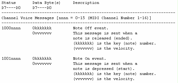
The site www.midi.org provides specification for MIDI as an open standard. A MIDI message is sent by a device (such as a piano) everytime an event occurs. The most basic events are "Note On" and "Note Off," which occur when a note is pressed and release, respectively. The digital data in the MIDI message sent for these two events is shown here, and the picture links to Table 1 on the midi.org website, which shows other basic messages.
WEEK 10 SUMMARY
Accomplishments: Submitted PCB and took a break. Began researching and experimenting with MIDI.
Weekly Work Total: 12.5 hr
Project Work Total: 159.25
Week 11
Monday October 29, 2007 (2.5 hr): Worked Individually with MIDI keyboard trying to analyze input, but didn't make much progress. Karl suggested using the oscilloscope across the MIDI connector. The signal has lots of noise and the information is difficult to capture. Using the Run/Stop button, I was able to view some 1's and 0's, but they don't match up with the data format for MIDI messages. I got a 4N33 optical isolator from the parts room and hooked up a circuit similar to the one in our schematic, but the 4N33 is not the same as the 6N137 optical isolator that we have in our circuit. I was unable to get any intelligible output from the optical isolator.
Tuesday October 30, 2007 (1.5 hr): Stopped by lab.
Curtis got out the actual opticalisolator that we're using on our board (which unfortunately is through-hole) and put it in the circuit and analyzed the output of the opto-isolator, which provided a clean digital signal. Tom figured out that the serial signal is transmitted LSB-first. We decided that the ossciloscope is probably the best tool for viewing the serial data package. I began recording some messages and found that they were 29 bits long. Tom was getting 19-bit messages for some reason; the only difference seems to be the horizontal scale used. His was about 5ms/div, mine was 100ms/div.
Wednesday October 31, 2007 (1 hr): Worked Individually.
I continued experimenting with the MIDI signal that is output from the keyboard. I collected some data:
Frequency: 31.25kHz Period: 32us
Push 47 @ 1ms/ with Single: 00000100110111101001001000010
Push 47 @ 100ms/ w/ Rn/Stp: 00000100110111101001011101000
Then Chuck helped me set up the Logic Analyzer and look at the signal on that.
Thursday November 1, 2007 (.5+2.5+.5+9:45-1:30am = 7.25 hr): Worked Individually.
Practiced soldering. When board arrived, I soldered the power jack, two headers and two capacitors.
Then I worked on the MIDI input for awhile. The following research was done:
Tests conducted @ 100ms/ w/ Rn/Stp
Push 53 (110101): 00000100110101011001000101100
Push 59 (111011): 00000100110110111001010000010
Push 61 (111101): 00000100110101111001000001100
Rel. 53 (110101): 0101011001000000000 - not sure why I got this result
Rel. 53 (110101): 00000100110101011001000000000 - redo of above test
Rel. 59 (111011): 0110111001001101010 at -318ms AND 0110111001000000000
at 412ms
Rel. 61 (111101): 0101111001000000000
Rel. 61 (111101): 0101111001000000000
Chords:
Push 60,64,67 (00111100,01000000,01000011): 00000100110001111001000010010 start at 293.0ms
then-------------------------------------: 0000000101001011010 start at 305.5ms
then-------------------------------------: 0110000101010001010 start at 309.3ms
Push 55,59,62 (00110111,00111011,00111110): 0000010011011101100101100101010110111001001011010 at -119.5ms
then-------------------------------------: 0011111001001100110 at -110.0ms
then-------------------------------------: 0101011001010101100 at -93.03ms
then-------------------------------------: 0101011001000000000 at -16.63ms
Push 64,68,71 (01000000,01000100,01000111): 00000100110001000101010100010 at 281.3ms
then-------------------------------------: 0000000101010100010 at 283.2ms
then-------------------------------------: 0111000101010111100 at 299.8ms
Analysis - done in tablet's Journal
Friday November 2, 2007 (4.75 hr): Met with team and worked individually.
I talked to Curtis and Tom about MIDI research I did last night to let them know what I learned and what still needs to be figured out.
I connected the power generator to 9V and put it on the pwr jack that I soldered last night. We are unsure about our 5V regulator right now -- we will probably order a new one with a higher power rating. I temporarily put the one we have in (its through-hole) and made sure that 5V is supplied to the header J7 and to some vias on the 5V plane. Then I talked to Karl about my plan for soldering the rest: I plan to put the 3.3V and 1.2V regulators on, then the MIDI jack and optical isolator, then the oscillator, and test each thing as I go. Then I can either solder a ton of caps in preparation for the FPGA and Serial Config, or I can work with the SRAMS.
I worked on soldering and got all of the power circuitry on and tested.
Saturday November 3, 2007 (5.25 hr): Met with Tom and Curtis.
We talked about the MIDI input for awhile but didn't make much progress. We looked through some open-source code for Synthesia, but their MIDI input comes through USB so it is coded differently. We added a .01uF capacitor to the MIDI input circuit to compensate for voltage spikes we had been getting on the edge of all of the MIDI signals, and that fixed the problem. We'll have to fly-wire a .01uF cap between the optical isolator and the level tranlator as a bypass to ground. (one lead on the line between opto-iso and lvl trans, the other lead grounded.)
I soldered the oscillator and nearby cap on, but there is something wrong. The voltage on the 5V plane goes up to 6.something now. I want to test the oscillator Monday without the rest of the board and make sure that it works outside the circuit before I put it on our board. (there is a spare I will work with.)
WEEK 11 SUMMARY
Accomplishments: Experimented with MIDI signal. Began populating PCB.
Weekly Work Total: 22.25 hr
Project Work Total: 181.5 hr
Week 12
Monday November 5, 2007 (4+1.75+5:45p-8:15 = 8.25 hr):
We had been having problems with the PCB since the oscillator was installed. After testing things with the DMM to make sure nothing was shorted, I looked at the datasheet for the oscillator and noticed that it calls for a .01uF bypass capacitor and our circuit has a .1uF polarized capacitor. I then supplied about 5V to the PCB input (which should eventually be 9V) and looked at some signals on the oscilloscope. (Supplying greater than 6V causes an audible ringing noise and fluctuation on the power planes. This is why I was testing with about 5V.) With a 5V input to the 9-to-5 regulator, the 5V and 3.3V planes were fluctuating with 400mV and 50mV peak-to-peak, respectively. At this point we noticed some other capacitor values on the circuit were not right; specifically I saw some capacitors around the DAC (a part of the circuit I worked on a lot) that had... 'unfamiliar' capacitor values. I looked at the DAC datasheet to be sure and confirmed that about half of the capacitor values near the DAC were wrong. This seemed (and still seems) very strange and unfortunate. I thought I could not have possibly screwed the circuit up that badly so I looked at our Design Review and found that snapshots of the schematic that we included in our Powerpoint presentation have the correct capacitor values. Conclusion: somewhere between the Design Review and when we restarted our PCB Layout a bunch of cap values got re-assigned, seemingly randomly. I don't know how or why it happened, but it has cost me about 8 hours to troubleshoot and fix.
After discovering this, I looked through other parts of the circuit, specifically around the power circuit that is already soldered and parts near the oscillator, and I found more values that are wrong, most notably C32 which is .1uF on the current schematic (and PCB layout) and was 22uF at the Review, and C38 which is 10uF now but used to be (back when it was correct) 100uF. I made these changes on the PCB (which involved a bit of desoldering and resoldering) and viola: the power planes are now stable with a 9V input, there is no audible ringing, and the oscillator is outputing a clean 80MHz clock signal. Disaster averted. Except we now have to re-examine all of the capacitors. And we should probably check the resistor values too.
I got the optical isolator on the PCB and was able to plug the keyboard into it and see output on the oscilloscope. tomorrow is the level translator... and hopefully lots more.
Tuesday November 6, 2007 (4.5 hr):
Forward progress on PCB soldering. I got the level translator and associated header and diode on, and I fly-wired a cap between the oscillator signal and ground to guard against voltage spikes on the MIDI input. I talked to Tom about the MIDI input, and he and I are going to work together on that and he'll supply the VHDL syntax knowledge and I will help with the logic.
Our serial config devices came in today so I put that chip on the board. We still need to put several caps on around the FPGA and then solder the FPGA on and test it.
Friday November 9, 2007 (3 hr):
Soldering: a couple capacitors were fly-wired and fly-wiring for a new 5 V regulator was begun. I also discussed software with Curtis and hardware progress with Vik.
Saturday November 10, 2007 (2hr):
Finished the fly-wiring for the new 5V regulator, then put it on the board and tested it. When testing the MIDI output from the board, I noticed that the periodic pulses often spike as low as -2.2 V. I'm not sure yet if this will cause problems for the FPGA. All other systems appeared stable: the power planes read accurately and the oscillator measured approx. 80MHz.
Saturday November 10, 2007 (3.75):
I discovered that adding a .1uF capacitor between pin 4 of the voltage regulator and pin 117 of the FPGA (same as pin 1 of header J8) removes the aforementioned -2.2V spikes on the MIDI input signal. (This should have been done instead of the .01uF capacitor that was added between pin 6 of the optical-isolator and pin 3 of the voltage regulator.) I added the .1uF cap and tested the circuit. The -2.2V spike was no longer there; the furthest the MIDI input dropped down was -60mV.
During the same test, I found that the oscillator's min/max values were 1.1V and 2.2V respectively. I checked the altera device handbook (Section I Ch. 5 P. 5 (Table 5-6)) and found that the Voltage input low is 0.8V and Voltage input high is 1.7V for logic 0 and 1 on any input pin. The FPGA may not interpret the current clock signal correctly. The oscillator data sheet, however, says that the output should range from .1*Vdd to .9*Vdd, which in our case with a 3.3V Vdd would be .33V to 2.97V. Before we realized the capacitor values on our schematic were incorrect (see Monday 11/5), we put a .1uF capacitor on C53, the bypass for Vdd on the oscillator. This capacitor should have been .01uF, and I suspect that this is the reason for the incorrect amplitude.
I replaced the .1uF in C53 with a 12000pF part from the parts cabinet, but when testing I found that the min/max had changed to 1.5/1.8V respectively. I found a prototype board of the oscillator and connected it with a .1uF and then a .01uF capacitor. I found that the capacitance didn't make much of a difference, but I also found that the min/max for that setup was about. 4V with a 3.3V Vdd, which might mean that that oscillator is bad.
WEEK 12 SUMMARY
Accomplishments: PCB population progress. Power circuitry, oscillator, optical isolator, and level translator are soldered.
Weekly Work Total: 21.5 hrs.
Project Work Total: 203 hrs.
Week 13
Monday November 12, 2007 (6 hrs):
During further testing I discovered that the reason the output of the oscillator was incorrect was because the probe was bad. With the .01uF cap in place and using a working probe, the oscillator output's min/max is 480mV/2.83V. With this working, the next step is to solder the FPGA. But first, here is data collected from a thorough testing of the current PCB configuration:
| With DMM: | 5V plane: 4.95V | 3V plane: 3.29 V | 1.2V plane: 1.19 V |
| MIDI (Scope over 100ms): | min: -30mV | max: 3.41V |
| Oscillator (with scope): | min: 550mV | max: 2.80V | freq.: 80.0+/-.2MHz |
I put the FPGA on the board and tested the PCB with the DMM. The 1.2V plane was shorted to the GND plane.
Monday November 12, 2007 (2.75 hr): Met with team.
Looked at FPGA on PCB under microscope and cleared out any potential solder-bridges or bad solder joints, but the 1.2V plane is still shorted to GND. We reviewed some of the pin information for the Cyclone II and tried to identify pins that are internally connected by probing a spare FPGA. We also reviewed the schematic and the PCB Layout looking for an error, but nothing has yet been found.
Tuesday November 13, 2007 (1.5 hr): Met with Chuck and with Tom.
In response to our problem with the 1.2V plane, Chuck had me clean the FPGA further using more flux-remover, a brush, and an air gun upstairs. This cleaning did not cause any change, so per Chuck's recommendation I started pulling up a couple suspect power and ground pins. When testing the plane, the resistance read about 58 ohms, and we were expecting an open circuit. Chuck then said that the 57 ohms we were seeing might be okay because that isn't really a short. Considering it further, 1.2V/50ohms=20mA, so with 58ohms we'd be seeing less than 20mA in the FPGA circuit, which seems tolerable. We tried hooking up power to the circuit and measured the current through the power supply. The current started below 1mA and then after several seconds jumped up to around 90mA, but circuit components did not heat up. I measured the voltage on each of the power planes and found them to be nominally close to their intended values.
Tuesday November 13, 2007 (4 hr): Worked with Tom and Vik.
Having sucessfully tested the voltage on each of the power planes with the FPGA on the PCB, Tom and I loaded a simple "heartbeat" program onto the FPGA. The program loaded sucessfully and we measured the signal of pin 188 on the scope, which was programmed to pulse with a specified frequency relative to the clock signal. The signal measured on the scope was what we expected, so the FPGA connection and the clock were verified.
With the FPGA in place, I soldered the rest of the periferal components for the DAC, included the ferrite beads.
I then tested the circuit:
| With Ag. DMM: | 5V plane: 4.973V | 3.3V dig: 3.313V | 3.3V ana: 3.307V |
| 1.2V plane: 1.1995V |
| MIDI (Scope over 100ms): | min: 20mV | max: 3.34V |
| Oscillator (with scope): | min: 920mV | max: 2.44V | freq.: 80.3MHz |
| FPGA Heartbeat: | min: -780mV | max: 3.84V | freq.: 30.3kHz |
With this testing done, I soldered the DAC to the board and checked everything again. The only major difference was found with the oscillator amplitude, which now has a max/min of -90mV/3.44V. This is approximately 1V difference on each measurement as compared to before the DAC was added. These levels are still acceptable, although it is strange that adding the DAC would cause that change. Testing it with a different probe yielded different results (min/max=160mV/3.16V, which is close to expected), so I believe the DAC is ready to be tested.
Tuesday November 13, 2007 (1.5 hr): Met with Tom.
Tested the DAC by loading a program to the FPGA that would just output green to the screen. Nothing happened, and there was no signal on the Blank pin to the DAC. The screen did come out of idle, but it remained black. We tied the reset pin high and the blank pin showed a signal, but the analog output of the DAC was still just noise near zero.
Wednesday November 14, 2007 (1.25 hr): Worked individually.
Reviewed DAC circuitry and compared it to the datasheet and to the schematic of the DE2 board. The only differences seem to be that the DE2 board uses a 5V input, but our chip is a 3.3V version, and the DE2 ties !PSAVE high and we tie it low. The DAC datasheet says the !PSAVE is just for a power save mode, so it doesn't seem like it would affect the output.
Thursday November 15, 2007 (3 hr): Worked individually.
I called Analog Devices last night to ask about the !PSAVE pin because I began to suspect that the "power save" mode was rendering the chip idle. This suspicion was confirmed by an Analog Devices technician. Chuck scratched the trace away and I connected it to power. With the !PSAVE pin high, the DAC will never go into power save mode now. We connected the monitor to the PCB and saw a white screen, as expected. I then soldered the SRAM and associated headers onto the PCB. I began looking for an enclosure for the project and started soldering the MIDI LSI.
Friday November 16, 2007 (3.5 hr): Worked individually. Reviewed the C code that Curtis has been working on to learn how it is structured. I briefly attempted to learn how interrupts are used in C by researching online, but not much was found. I searched for enclosures on digikey and limited the search to one of these enclosures. I recorded some ideas for the C code in the Microsoft Journal.
Saturday November 17, 2007 (1 hr): Worked individually.
Developed MATLAB code that can be run to convert any image into a black and white image represented in binary, where for each pixel a 1 is assigned for white and 0 for black. This will assist in generating further text and graphics for the environment the user sees. I then spent a good deal of time experimenting with other options. I was not able to figure out how to get color data in hex without converting every pixel individually. I also had trouble writing the binary representation of the image to a file, but it can be done pixel-by-pixel. For a small binary image, this is okay, but for large images or for color (where there are three numbers (RGB) for each pixel), MATLAB takes too long to process it. It will probably be easiest to just copy all of the binary information out of MATLAB to the clipboard and then paste it into the project, or if necessary into a text file for further editting.
MATLAB code:
clear all, clc, close all, imtool close all
pic = imread('alphabet.bmp');
sizea = size(pic)
bw = im2bw(pic,graythresh(pic));
figure, imshow(bw);
a=bw(13:37,10:24)
figure, imshow(a);
Input:

Output binary:
Excel file
Saturday November 17, 2007 (2.5 hr): Worked with Curtis.
Worked trying to load C program onto our board. Up to now all C development has been done on the DE2 board. Last night there were problems communicating with the SRAM on our board, but that problem was resolved this morning. Now the problem is with loading to the Serial Configuration Device. There are several ways of transferring software onto the Serial Config, including Active Serial Connection, Passive Serial Connection, and JTAG. We designed our board for Active Serial Connection and have been able to use that to load everything that is controlled by the VHDL. Loading the C program will require using JTAG. There are four pins that we tied either to power or ground that we now need access to in order to use JTAG, specifically pins 22-25 of the FPGA. Pin 25 is a no connect, pins 22 and 24 are traced outside the FPGA to power. For these pins, a wire can be soldered to the pad and traces can be etched away as needed. The trace for pin 23 goes underneath the FPGA and is not accessible. For this pin the best solution seems to be to lift the pin off of its pads and solder a wire to it. The wires from these four pins can then be brought to a header. We have considered cutting the traces to header J12, tying the wires to that header, and using that header for programming.
Sunday November 18, 2007 (2 hr):Met with team.
I discussed the JTAG Communication method with Curtis. After determining that we really did need JTAG communication, We discussed the best way to modify the board to allow JTAG communication.
I also looked at the code Tom has been working on and watched him work in order to start developing an understanding of the VHDL portion of the project.
WEEK 13 SUMMARY
Accomplishments: Major population of the board, including troubleshooting for oscillator circuit, soldering and troubleshooting for the FPGA, the DAC, and the MIDI LSI. Became familiar with the VHDL and C codes that Tom and Curtis have been working on. Developed MATLAB code to create binary sprites.
Weekly Work Total: 29 hr
Project Work Total: 232 hr
Week 14
Monday November 19, 2007 (8 hr): Worked individually.
I reviewed the JTAG Configuration (from the FPGA datasheet) and drew a small schematic for how the FPGA and the header should be arranged:
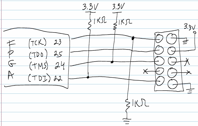
I talked to Chuck about implementing this. Pin 23, which goes underneath the FPGA, will be a problem, but we may be able to lift that pin off the pad and connect a wire to it.
This afternoon Chuck modified the board and soldered wires to pins 22-25 of the FPGA. I hot-glued a header to the board and Vik soldered the wires per the schematic I made. JTAG communication has not yet been tested, but the circuit has been created on our board.
I watched Tom work for awhile and assisted with logic for making the menu screen advance to the gameplay screen upon input from the keyboard. Several timing errors have impeded progress, and the screen still does not advance when a key is played.
I worked with Curtis for awhile. Having already reviewed his code on Friday, I was familiar with how it works. Tonight Curtis was able to successfully play the first 20 notes of Bubble Bobble through the MIDI LSI on a set of speakers. Right now the C code calls two seperate functions for audio and video. The first function plays the notes over the speakers, and the second function creates the bars that scroll down the screen. These things need to happen at the same time, so they cannot be two sepearte functions called sequentially. Curtis and I then began discussing how best to combine these two functions. Curtis had the idea that we could send each note to the FIFO buffer on the MIDI LSI as it hits the bottom of the screen. Another idea I came up with is sending notes to the MIDI LSI FIFO buffer as the bar for the note is generated. One problem with this is that whenever there are more than about twenty notes on the screen at once, we would over-run the buffer. Through discussion Curtis and I came to the idea that we could start by filling the buffer to capacity before the song is played and increment a counter for every note that is put in the buffer. Then as the song plays, the hardware could indicate when notes hit the bottom of the screen. A counter would keep track of how many notes are in the buffer and would decrement every time a note hits the bottom of the screen. (Presumably the note is played on the speakers and leaves the buffer at that point.) Then in the same loop that creates the bars we would check to see if the counter is less than the maximum the buffer can hold, and if it is, more notes would be loaded to the buffer and the buffer would increment for each note loaded until the buffer is full.
Tuesday November 20, 2007 (14 hr): Met with Curtis.
We discussed several methods of writing a function that would create bars on the screen and simultaneoulsy manage the task of sending notes to the small MIDI LSI FIFO buffer. We were concerned with the delays that would accumulate due to overhead in the code, so Curtis used the oscilloscope to monitor the serial signal that is sent over the SPI to write a note to the buffer. The note consists of six data packets and takes a total of 163.6us. This is a problem because the code currently uses the usleep function to 'sleep' until the next bar needs to be created, and it takes care of all the other operations in between calls to usleep. Effectively, the bars will trail the audio by the accumulated delay that comes from those other operations. I looked at some sheet music that I brought into lab for the song 100 years. The song is ten pages long and has 134 notes on the first page. If the first page is a good average, the song has about 1340 notes in it, so by the end of the song the bars will trail the audio by 219ms due to the time spent sending notes to the buffer.
Sunday November 25, 2007 (30 min.):Met with Tom.
Tom and I talked about project enclosures and about the scoring algorithm for evaluating the user's performance. I looked for enclosures in stores this weekend and bought the best one I found, which was 10"x10"x4" at Home Depot. Tom found a good one online that he ordered tonight. Tom changed the score bar so that its color depends on how high the score is. It turns red for a low score, green for a high score, and yellow in the middle. We need to work on the tolerance for letting go of a note because right now it has to be pretty exact in order to get a good score.
WEEK 14 SUMMARY
Accomplishments: Designed a modification to allow JTAG communication. Worked on C code to synchronize the song playing (audio) with the bars falling (video). Found project enclosures.
Weekly Work Total: 22.5 hr
Project Work Total: 254.5 hr
Week 15
Monday November 26, 2007 (6.5 hr): Met with Tom and Curtis
Altera responded to us about JTAG/Active Serial communication and told us about a way of combining the VHDL and C codes into one file that can be loaded via Active Serial communication. Curtis loaded the file onto our board, but the software is never prompted to start running, so the whole system doesn't do much. He submitted another help ticket regarding how to start the C code.
Curtis and I worked on the C code. Timing errors were coming from the fact that some of the delta_t's (which indicate how much time elapses between note on/note off instructions) were larger than the one-byte maximum the LSI requires. Curtis had attempted this problem last week by inserting "no-op" commands in the notes list, but his code wasn't creating enough no-ops. We changed the way it creates the nops so that it creates a long enough delay.
I made some more sprites, including an example song list, the alphabet, and a title for the song list. Tom put them into the VHDL. We are runnning low on logic gates, so some sprites may need to be minimized.
Tuesday November 27, 2007 (3.5 hr):
Made more sprites to include in the "Song Complete" screen and "Song Selection" screen. I talked to Tom about a way to create a break between consecutive notes of the same key, which we will likely implement tomorrow. I also watched Curtis trying to get the NIOS working so that we can program our board.
Wednesday November 28, 2007 (3 hr.): Met with team.
After our Progress Briefing, I read the Service Request that Curtis has been maintaining with Altera. I tried calling Altera but needed an Altera ID to proceed. Dr. Johnson was able to provide me with an Altera ID during his office hours. By that time, however, Vik had made a breakthrough. We had been programming correctly, but we needed to remove the programming cable after programming and before running. After doing this, we were able to run the code on our board for the first time. Vik also found that the audio jack footprint was wrong, so some pins were mis-connected. I soldered two headers onto the board and fly-wired the audio jack, which Curtis had de-soldered and hot-glued to the board.
Thursday November 29, 2007 (1 hr): Worked individually.
Worked on user manual. Specifically, I read some past User Manuals for style ideas and re-wrote the Product Description portion of our manual. I then worked on the Product Illustration. We need to take updated screen shots of the game screen and a picture of our packaging.
Friday November 30, 2007 (1.5 hr): Worked with team.
Finished user manual. Tom took pictures of the jacks on our PCB and I pasted them onto a picture of the packaging of our project, then made callouts to describe each jack. Tom and Vik made notes for the content of the troubleshooting section and I typed the information into the user manual. The other sections were finalized, and the final document is available on our documents page.
Sunday December 2, 2007 (3.5 hr): Worked with Tom and Curtis.
Tom and I modified the VHDL code to create a line between consecutive notes of the same key so that they don't appear as one note. The C program provides an input array that tells the VHDL which positions bars are being created in. When a key is played more than once without a break, the note off message for the first note and note on message for the second note occur in short succession and the two notes appear as one big note. Effectively, the new logic we wrote latches the 0 from the input when the note off message occurs, and it doesn't record the 1 caused by the note on message until the 0 has been propogated down and a black line appears between the notes. Every time the bars on the screen get propagated down, the current status of the array from the C program is copied into the top row of the barmap matrix. In between propagations, the top row of the barmap matrix is ANDed with the current status.
WEEK 15 SUMMARY
Accomplishments: Made sprites for on-screen graphics, completed the User Manual for the project, and developed and helped implement logic for the VHDL code to display a line between consecutive notes.
Weekly Work Total: 19 hr
Project Work Total: 273.5 hr
Week 16
Monday December 3, 2007 (9:30 - 10:45, 3:30 - 4:20, 5:15 - 7:45, 8:15-1:15 = 1.25+1+2.5+5= 9.75): Worked individually.
I reviewed the guidelines for the Final Report and began editting HW3 for inclusion in the Final Report. I am not sure how much we are supposed to edit the homeworks to account for things discovered or changed since the homework was first submitted. In HW3 we account for a USB device which was not implemented in our project.
I looked over the Quartus II project on my own to understand the structure of the project. Before now I have been helping with the C code and VHDL logic, but the process of compiling those codes and coordinating the hardware and software on the chip has been done by Curtis. I looked at the SOPC builder, the MIDI_Parse_Sch.bdf window and the MIDI_Parse.cdf window and started to see what each piece is doing. When Curtis got here he explained how things fit together. The C code is developed in the NIOS environment and "built" into a .elf file. Then the SOPC Builder is used to convert the .elf file into a hex file. The MIDI file being used is also converted to a hex file. The VHDL is made up of several files. In Quartus II, the MIDI_Parse_Sch.bdf tab
shows the dependencies between the files and the information that is shared by files. These files are compiled into a .sof and a .pof. The .pof can be loaded onto the board to run just the VHDL code. To run the entire project, we compile the .sof file and the two hex files (the one that started out as the C code and the one that started as a .mid file) into a .pof and load that .pof onto the EPCS serial config device via Active Serial communication.
We dealt with several problems today. First, the keyboard region on the screen was distorted. We're not sure exactly what fixed this problem, but we changed the SPI setup and it worked, then we changed it back and it still worked. Some of the lines between the white keys were not appearing, but that problem also went away next time we compiled the project.
The MIDI LSI chip on our board did not work at all before today. We have an LSI chip on a prototype board that we had connected to the DE2 for testing and development. In order to debug the chip on our board, we connected the LSI prototype board to our PCB through a spare GPIO header. We noticed in the DE2 schematic that there are 47 ohm resistors on each pin leading from the DE2 to the header pins we've been connecting the MIDI LSI to, so we added resistors in between the header and the LSI, but we still didn't have any audio output. We then tested all seven signals that are output to the LSI from the FPGA, both on our PCB and on the DE2. We compared these signals and found that for six of the seven signals sent to the MIDI LSI, our PCB behaves the same as the DE2. The SCLK, however, was a different frequency (10MHz on our board and 13.333 MHz on the DE2). We changed the way that the clock is assigned and the audio worked on our board for the first time.
Tuesday December 4, 2007 (2:15-3:30, 5:30-6:15, 8:30- 3a = 8.5 hr): Met with Team.
This morning we demonstrated our PSSC's. All five were demonstrated successfully. After demonstrating, we began to modify the project and add enhancements not required for the PSSC's. First we wanted to go back to using the MIDI LSI chip that is on our board instead of the one on the prototype board. We tested the prototype board without the resistors we added and no sound output was generated. From this we learned that the resistors are necessary and we cannot use the configuration on our PCB. It would be very difficult to flywire resistors into that part of the PCB, so we decided to attach the MIDI LSI on the prototype board to our PCB via a GPIO header. Audio output pins on the FPGA were then reassigned to that header and the MIDI LSI prototype board was integrated with our PCB.
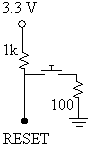
| Tom bought a pushbutton from the HKN Parts Room for the Reset pin on the FPGA. The button is normally open and shorts on push. We want the Reset pin to be normally high and ground on push. We designed the circuit shown at right to accomplish this. |
 |
I made new sprites for the song selection screen that contain the actual names of the songs we used in the project. Meanwhile Curtis noticed that the music becomes unsynchronized with the bars near the end of both songs we're using. We noticed that it seems to happen on a specific note near the end of each song, but the note did not seem unique in anyway that might make it cause a delay. We worked on debugging this issue on the DE2 but did not solve the problem yet. We also tried to find .mid files online for songs we can load onto the game. I found several that could work and I found a program that removes tracks from MIDI files so that we can remove drum and vocal parts when we want to. We had some difficulty loading these songs into the game because they did not follow the format expected by our MIDI parsing function.
Wednesday December 5, 2007 (2 hr): Worked individually.
Worked on Bonus Presentation and Final Report.
Thursday/Friday December 6/7, 2007 (19 hours): Met with team.
Worked individually on the Final Report. When Tom and Curtis arrived I spray painted the enclosure and we put some finishing touches on the project in hardware and software. Tom and I worked on planning the movie and found some effects to use in iMovie.
We met later that night in Hillenbrand to film the movie. When we got done filming we editted the movie in time to show it to 270 and 362 that afternoon.
Sunday December 9, 2007 (14.5 hours): Worked individually on final report.
Later met with team and finished Final report and other documentation to be turned in Monday December 10.
WEEK 16 SUMMARY
Accomplishments: Demonstrated PSSC's, put project in enclosure, demonstrated project in TSCP session and in ECE270 and ECE362, completed Final Report and documentation.
Weekly Work Total: 44
Project Work Total: 317.5 hr