CMOS+X Nanokernels and Nanosystems
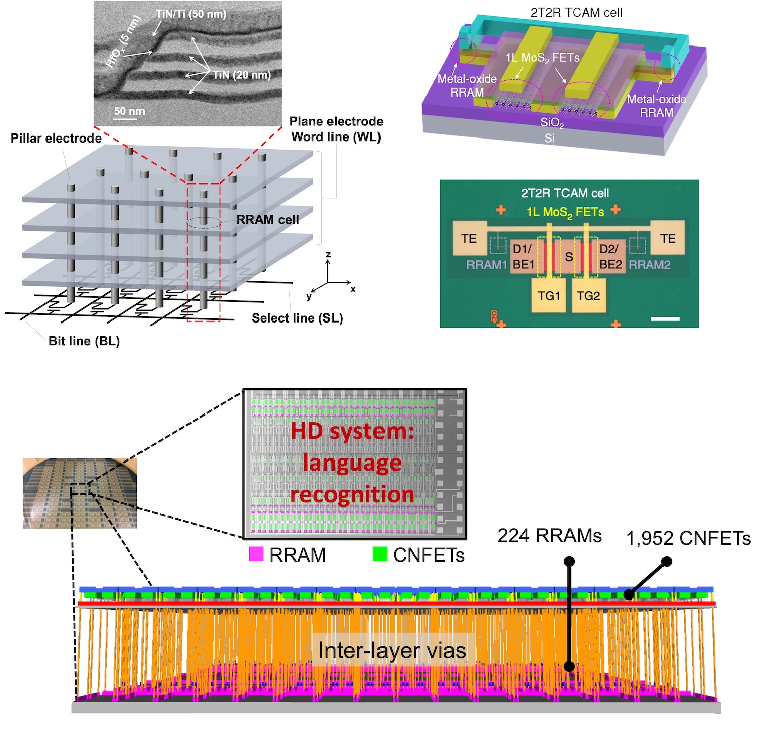
3D integration of new nanotechnologies and silicon CMOS enables energy- and area-efficient implementations of new compute kernels and system-on-chips. These building blocks can be further packaged into heterogeneous systems for heterogeneous applications.

There is plenty of room for technology advancement beyond miniaturization: the vast design space offered by new physics, new materials, and new devices can lead to a high density of nano-kernels and nano-functions for a computing system, augmenting today’s leading-edge logic technologies for broad societal impact. Exposing this rich design space at the bottom to the cross-layer design explorations of new AI hardware requires a solid experimental foundation, so that device experimental and theoretical research on the one hand, and circuit integration/optimization on the other hand, form a closed loop to accelerate innovations and translation to practical technologies.

We are working on:
- High-density 3D memories with charge-based, resistive, and ferroelectric devices.
- CMOS+X integration with BEOL-compatible oxide semiconductors and 2D materials.
In the previous collaborative work, various nanoscale memory and logic devices (planar and vertical RRAMs, silicon FETs, 2D material sheets, 1D nanotubes) are monolithically integrated, revealing unique device-level functionalities enabled by new materials into upper layers of system abstraction. With certain functions directly realized within compact “nanokernels”, we further show taht the integration of nanokernels provides interesting synergies that lead to efficient “nanosystems”.

Related publications:
IMW 2025, IEDM 2024, Nature Electronics 2019, ISSCC 2018, JSSC 2018, IEDM 2017, VLSI 2016