Experimental collaboration for ultra-scaled FETs
One of the important aspect in the group is to apply theory to explain the experimental results. Over the years many experimental results have been successfully understood and explained using the quantum transport theory and the simulators developed in the group. Below we outline the important projects.
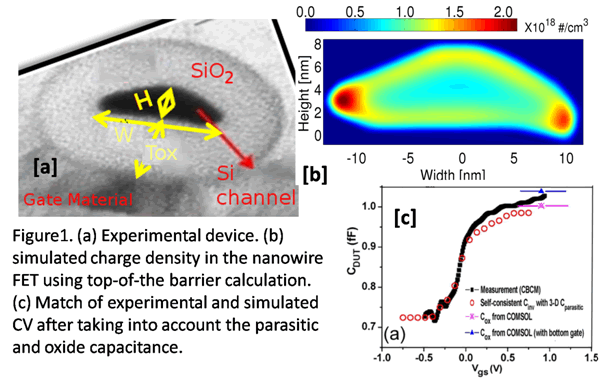
CV calculation in Nanowire FETs ( with IME Singapore):
This work was done in collaboration with IME Singapore and Purdue University. IME Singapore provided the experimental CV results which were benchmarked using the charge self-consistent calculations implemented in Bandstructure Lab as shown in Figure 1.
 More details on this project can be found here
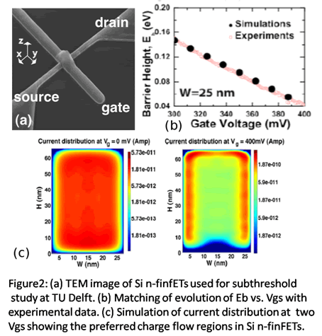
Subthreshold transport in Si-FinFETs (with TU Delft, Netherlands):
This work was done in collaboration with Prof. Sven Rogge from University of New South Wales, Australia (in the past at TU Delft, Netherlands). The work involved understanding the evolution of source to channel barrier (Eb) and active cross-section area (S) with gate bias in intrinsic channel Si n-finFETs done at TU Delft. The devices were fabricated at IMEC ,Belgium. At Purdue we explained the evolution of Eb and S using the self-consistent calculations and in the process also determined two new methods to calculate the interface trap densities in state of the art Si n-finFETs. More details about this project on this page
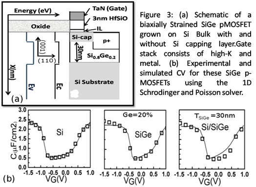
CV of SiGe pMOSFETs (with IIT Bombay/Sematech):
This work involved the calculation of CV in biaxially strain SiGe p-MOSFETs fabricated at Sematech, Albany, NY. The team from IIT Bombay measured the CV which was benchmarked using the 1D quantum simulator developed in the group which could easily take into account the strain and wafer orientation based on Tight-Binding calculation. More details on this page:
Group member involved:
Associated publications:
- Characterization and Modeling of Subfemtofarad Nanowire Capacitance Using the CBCM Technique, Hui Zhao, Raseong Kim, Abhijeet Paul, M. Luisier, G. Klimeck, Fa-Jun Ma, S.C. Rustagi, G.S. Samudra, N. Singh, Guo-Qiang Lo, Dim-Lee Kwong, IEEE EDL, Vol. 30. No.6, 2009, DOI : 10.1109/LED.2009.2015588
- Thermionic Emission as a tool to study transport in undoped nFinFETs, Giuseppe C. Tettamanzi, Abhijeet Paul, Gabriel P. Lansbergen, Jan Verduijn, Sunhee Lee, Nadine Collaert, Serge Biesemans, Gerhard Klimeck and Sven Rogge, IEEE EDL, 2009., DOI: 10.1109/LED.2009.2036134
- Interface Trap Density Metrology of state-of-the-art undoped Si n-FinFETs, A. Paul, G. Tettamanzi, S. Lee, S. R. Mehrotra, N. Collaert, S. Biesemans, G. Klimeck and S. Rogge, IEEE EDL, 2011. DOI: 10.1109/LED.2011.2106150
- Interface trap density metrology from sub-threshold transport in highly scaled undoped Si n-FinFETs., Abhijeet Paul, Giuseppe Carlo Tettamanzi , Sunhee Lee , Saumitra Raj Mehrotra , Nadine Collaert ,Serge Biesemans , Sven Rogge , Gerhard Klimeck, under review, JAP, 2011.
- Intrinsic Reliability improvement in Biaxially Strained SiGe p-MOSFETs, S. Deora, A. Paul, R. Bijesh, J.Huang, G. Klimeck, G. Bersuker, P. D. Krisch and R. Jammy, IEEE EDL, 2010.. DOI: 10.1109/LED.2010.2099101