Week 2
Date:
1/19/2017
Total Hours:
5
Description of design efforts:
- Facilitated development of a more compact functional model of our project.
- Purchased Udemy course and begun to familiarize myself with microcontroller.
- Learned the functionality of different sensors and used that knowledge to start thinking baout mechanical constraints and housing design.
Week 3
Date:
1/26/2018
Total Hours:
6
Description of design efforts:
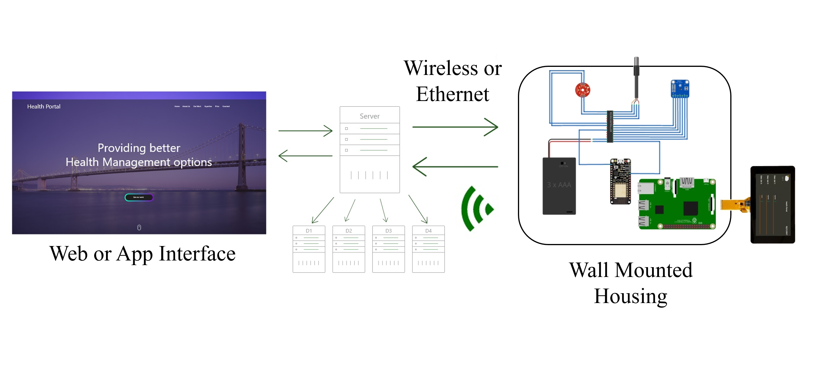
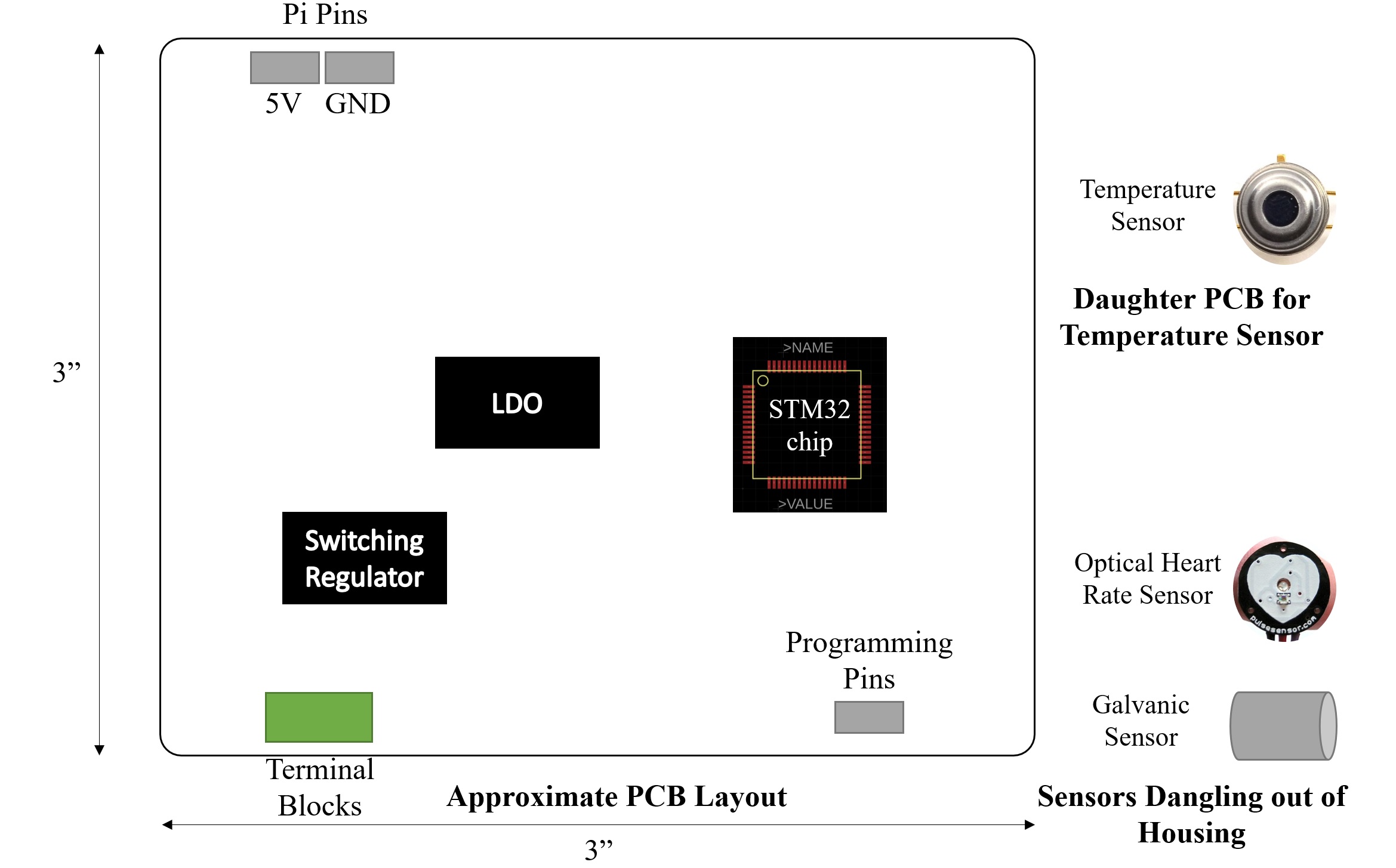
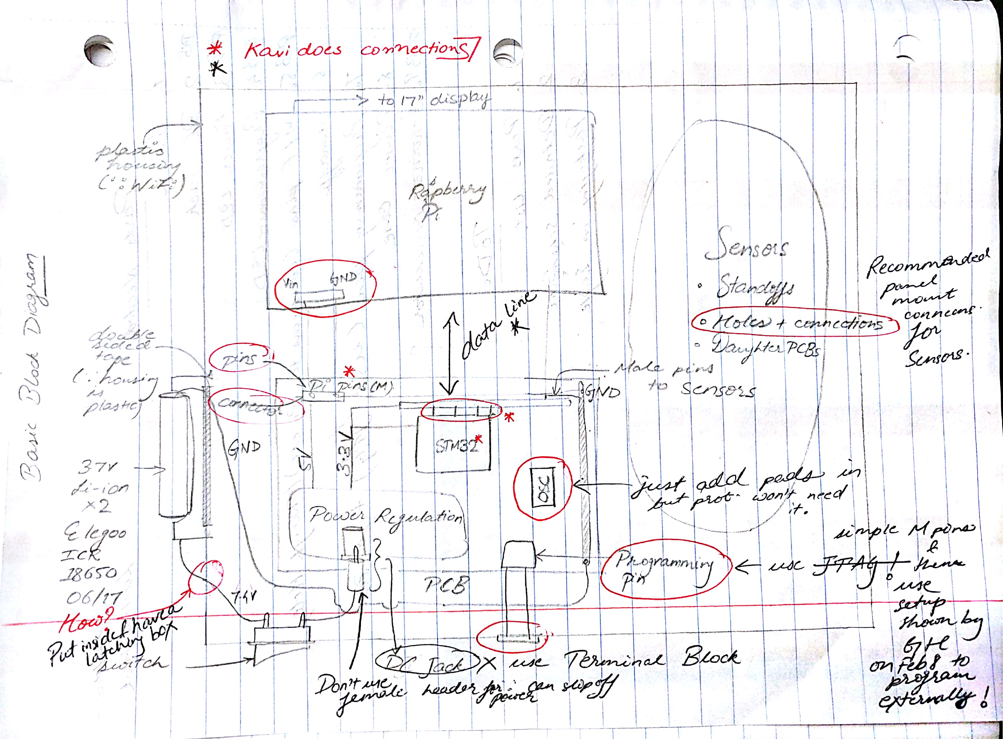
My main focus this week was to develop a clear image of the system level working of the project. Because this is primarily Asheem’s brainchild, it has been difficult for everyone to have a synchronized understanding of the block diagram. Furthermore, because I will be designing the housing and laying out the hardware, it is important for me to determine final part placement. As a result, it was important for me to drive a discussion about exactly how our components will be wired.
I proposed that we use one compact housing for the microcontroller, the battery and the raspberry pi, with attachments for the sensors that we will be using. All the connections within this casing will be wired. In a Production model, this casing will be mounted to the walls like a router and will transmit sensor data to the internet either via WiFi or via Ethernet. I proposed that we try to get the Ethernet working first as WiFi is harder to code. This transmitted data will be displayed as a graph on the HealthPortal website. Alternatively, we could program an app in the future if we have the time.
I made a block diagram of my design to make sure everyone was on the same page. Because of the effort I drove and the questions I asked, we could reduce our project complexity and leave room to add more functionality.
Proposed Layout
Week 4
Date:
Friday, Feb 2, 2018
Total Hours:
9
Description of design efforts:
| # | Issues | Resolution |
|---|---|---|
| 1 | Couldn’t figure out how to install libraries | Done using Resource 1 |
| 2 | Error while setting serial port parameters: 9,600 N 8 1 | Started working after fixing 4 |
| 3 | avrdude: ser_open(): can't set com-state for \\.\COM3 | Went away itself and got 4 instead |
| 4 | avrdude: ser_open(): can't open device "\\.\COM4": The system cannot find the file specified. | Changed to COM4 and re-plugged USB |
| 5 | Temperature and humidity readings are 0 | Connected to Oscilloscope and DMM, getting 5V output from Pin 2. Read some more documentation on Google. Try to get analog / digital voltages from sensor – 1. Print values from chk variable – chk is always -3 2. See DHT.read22 documentation a. Changed read22 to read 3. Changed data pin on Arduino from 7 to 2 after re-reading schematic on Resource 1 a. Chk now prints 0 (happens with both read22 and read) Solution – change data pin from 7 to 2 and change read22 to read |
1. http://www.ardumotive.com/how-to-use-dht-22-sensor-en.html
2. http://howtomechatronics.com/tutorials/arduino/dht11-dht22-sensors-temperature-and-humidity-tutorial-using-arduino/
B. VALIDATE SENSORS
- Housing needs to be redesigned
- Sensor takes a LONG time to get to body temperature levels
- 2 seconds per reading
- 0.1/0.2 degrees C rise per reading
- Temperature does not get to exactly body temperature
- This might be because of air gap in current housing design
- Need a beep to indicate end of reading
Alternate Sensors recommended -
| Recommended Temp Sensors | Recommender | Benefits |
|---|---|---|
| MAX30205 | Asheem (see if available on Octopart) | We can use the Fever Click design - https://www.mikroe.com/fever-click |
| MLX90614 (Infrared) | Asheem (see if available on Octopart) | |
| Thermistors | George Hadley (see if available on Octopart) |
Week 5
Date:
Friday, Feb 9, 2018
Total Hours:
17
Description of design efforts:
- PLAN (CHRONOLOGICAL)
- Watch YouTube videos to get familiar with the Eagle UI
- Design something on Eagle for practice
- Understand what needs to be on our PCB by looking at datasheet and look for components that need to be ordered
- Meet with Jeff
- Show what I made today on Eagle
- Verrify the components that need to be ordered
- Find a PCB vendor and try to place an order ahead of time / see what is required
- Get started on designing a schematic and laying out pads
- Draw housing on paper
- Find CAD tool by emailing George or Prof Thottethodi
- ISSUES FACED
- GLOSSARY OF TERMS / THINGS TO UNDERSTAND FROM OH
- RESOURCES
- LESSONS LEARNED (DESIGN PHILOSOPHIES)
- Place components on PCB to enable smallest connection lengths.
- Try to design PCB with least number of vias possible.
- PCBs can have different layers, and intermediate layers can be used for ground or power. 2 layer PCB means 2 copper layers.
- "Air wires” are connections between components drawn by Eagle to mimic the wiring in the schematic on the PCB.
- "Ratsnest” button – calculates the shortest distance between the components (“air wires”)
- PCB DESIGN CHECKLIST
- Make Schematic
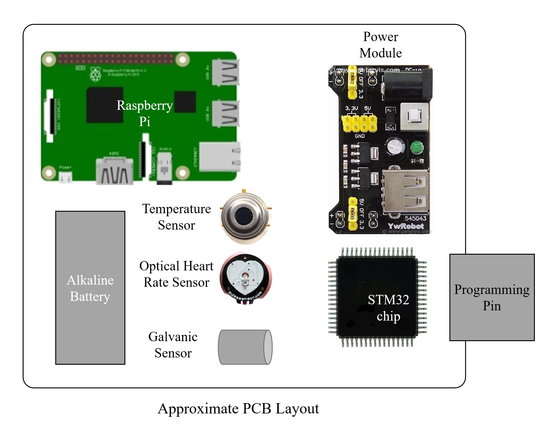
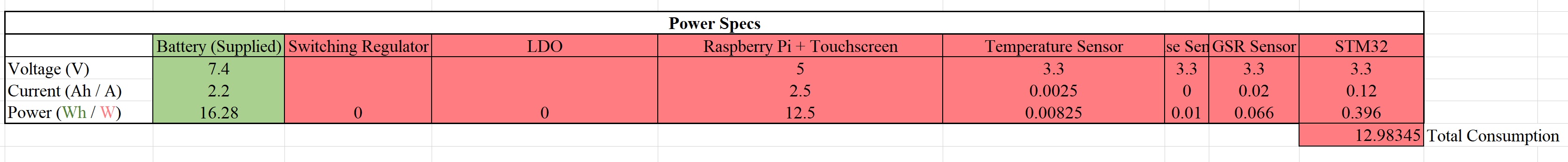
- Decide Parts based on Power consumption Excel
- Refine based off of physical dimensions of boxes
- Lay out as functionally necessary
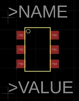
- Make custom footprints / packages as necessary
- Make footprints using Fig 38
- Lay out silk screen on tPlace – move behind pads
- Lay out finer silk screen in yellow on tDocu – move behind pads
- Click on text tool and type >NAME on tName and >Value on tValue – done
- Save and start a symbol drawing
- Draw a rectangle or whatever suitable shape
- Draw pins using lines and label pins wrt chip
- Place >Name through text option on Names layer
- Place >Value through text option on Values layer
- Change pin types (io, power,…)
- Make device
- Turn on relevant layers
- Move parts to preferred locations
- Press Ratsnest button to define shortest paths
- Re dimension board. Turn grid on if necessary to do so
- Define a ground plane (acts as a heat sink, ground plane, RF emissions)
- Hit Ratsnest to connect to GND plane
- Clean up the silk screens if necessary
- ATTACHMENTS
| # | Issues | Resolution |
|---|---|---|
| 1 | Unable to pan Eagle frame | Press down on mouse scroll wheel and move |
| # | Issues | Resolution |
|---|---|---|
| 1 | Can’t install stuff on Group computer – Specifically, STM32CubeMX (software to configure peripherals and creates a template to program the microcontroller: http://www.st.com/en/development-tools/stm32cubemx.html) |
Enter login credentials |
| 2 | What does this mean? “Note the THM package has the ground pads on both sides of the PCB so that the masks are the same - this reduces the cost.” ) | Idk but it is not relevant |
| 3 | What is a package, a footprint, and how do I know which one to choose in Eagle? | It is the “shadow” of a part that defines the physical characteristics of the part body. Eg. LQFP64 L – dimensions QFP – type, like BGA 64 – # of pins |
| 4 | Passive components (C0805, US375-192X418) nomenclature in Eagle libraries and how do I know which one to use? | Read the description and make a judgement. Eg. 0805 refers to the size of the pad |
| 5 | How to make the design I need to make and then validate it before sending it for PCB fab (and later getting a board that does not work!)? | Can’t validate a full schematic since of computation limitations. |

Note: CAD Designs are in Progress. I have made the STM32 device library on EAGLE (seen in picture above) and will upload the schematics next week when circuit connections have been finalized and PCB has been sent for fabrication.
Week 6
Date:
Friday, Feb 16, 2018
Total Hours:
7
Description of design efforts:
- STUFF I'M CONFUSED ABOUT
- PCB COMPONENTS THAT NEED TO BE CLARIFIED
- CHOICE OF FUEL GAUGE IC
- RESOURCES
- ATTACHMENTS
| # | Issues | Resolution |
|---|---|---|
| 1 | Plastic Housing can be warped by dremel | Use ABS Plastic and smoothen with knife |
| 2 | Measure Battery Voltage | Use a fuel gauge IC which has a high-resolution ADC (higher than STM) and an encoded lookup table and can send stuff to STM. |
| 3 | Interface fuel gauge IC with STM | Happens via I2C |
| 4 | Validate PCB | Test as many components as possible on breadboard first |
| # | Component and Question | Resolution |
|---|---|---|
| 1 | 1206K or 1206 capacitor? | |
| 2 | L_1206 value can’t be changed to 4.7 uH | |
| 3 | Where to get footprint for battery? |
| # | IC | Resolution |
|---|---|---|
| 1 | DS2782 | 1. Right package 2. Easy to solder on 3. Does not have enough voltage rating |
| 2 | TI BQ294522DRVT | 1. Meets electrical specs 2. Package available on and downloaded from DigiKey 3. Too small / hard to solder 4. I DON’T UNDERSTAND HOW TO MEASURE 5. Short V3 pin to V2 for 2 cell configuration |
| 3 | DS2781E+ | Seems okay as of now. |

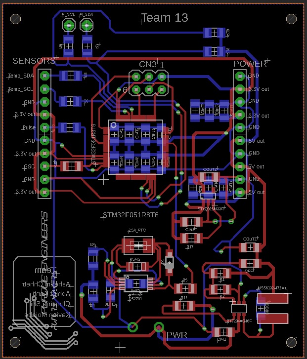
Power Regulation Schematic
STM32 IO
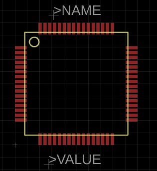
STM32 Footprint
Power Regulation IC Footprints
Week 7
Date:
Friday, Feb 23, 2018
Total Hours:
8
Description of design efforts:
As a result, there are not many report-worthy details, except a final selection of items that anyone who is replicating our project can use.
I’m still finalizing our board design (should be complete on Saturday), so no update there as of right now (Friday night).
Fuel Gauge IC was chosen - DS2781E+
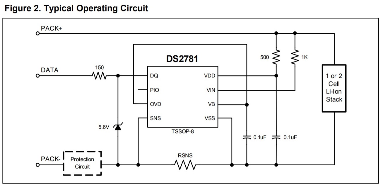
Fuel Gauge IC Schematic
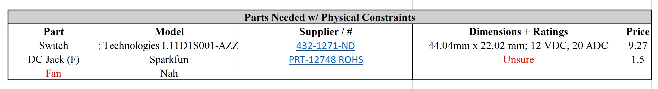
Terminal Block for Power Supply - Phoenix Contact 1729128 (1.3 mm hole diameter)
Housing Layout
ISSUES:
Week 8-9
Date:
Thursday, March 8, 2018
Total Hours:
25
Description of design efforts:
- Place decoupling caps as close to STM as possible.
- Use Figure 8 on Switching Regulator Datasheet for board layout.
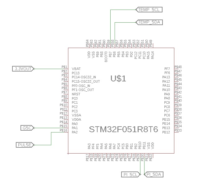
- Where does 1-Wire “Data” line go to from the Fuel Gauge IC to the STM?
- Pin 42 of STM according to Kavi <- STILL NEEDS TO BE CHECKED!
- Does changing pin type to I/O or Supply in package matter?
- No (according to Jeff).
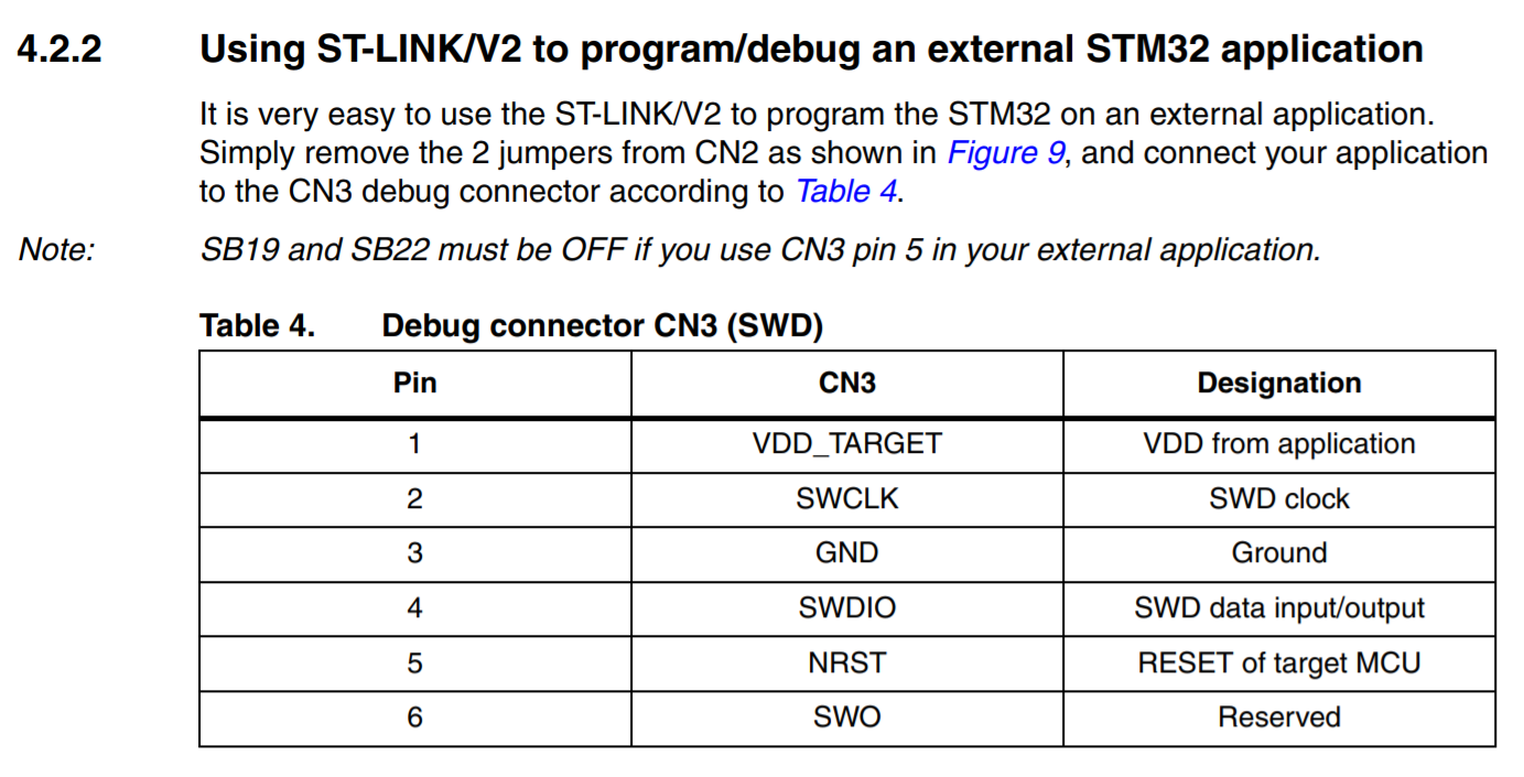
- Where are the programming pins on the STM?
- See Table and Schematic below.
- How to choose decoupling cap values?
- Standard or from STM Discovery PCB layout.
- Where do I connect EN pin?
- Vin via 100k on Regulator. Vin on LDO.
- What kind of PTC to use?
- Extra Power / Ground pins can be used for connecting LED to indicate power on / off.
- Add headers to 7.4V rail from battery as well (if asked to, or if deemed necessary).
- Place STM in center; place passives behind – how to place components on bottom layer
- See if I need an oscillator - NO
- Decoupling caps + power sources on bottom layer
- Prevent caps shorting
- Thickness of traces needs to be same as thickness of pads
- Trace needs to enter perpendicular to pads
- Make power trace thicker to 20-24 mils
- Avoid traces going directly underneath ICs, have them go on the flip side
- Traces must enter straight into pads and not at an angle (only like Pin 3 of SR)
- See if I2C for Raspberry Pi has a pull up resistor – Yeah, added 4.7k (thought not visible in Pi schematic)
- See PCB Resources in Course -> Processes
- Decoupling caps for STM must be taken as specified in datasheet – Done using STM IC sch.
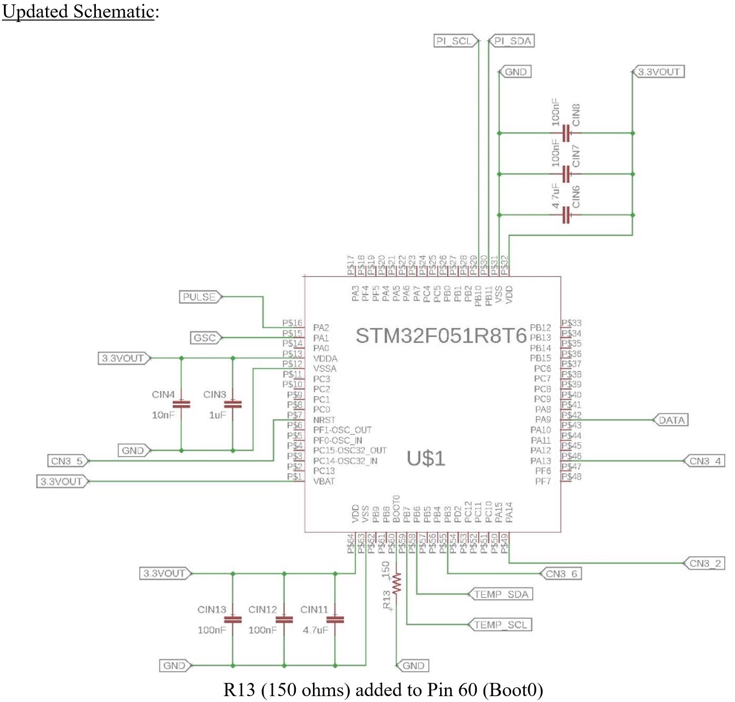
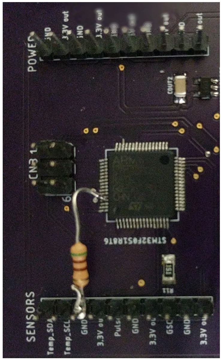
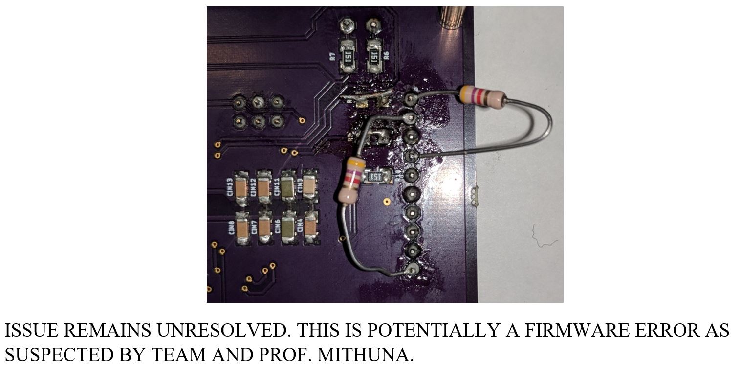
- Add small resistors for pins – Added 150 ohm.
- Make 4.7k in parallel with SDA/SCL in accordance with I2C convention on Temperature Sensor daughter PCB – Done and ordered by Asheem
- Make board smaller.
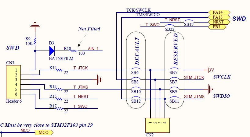
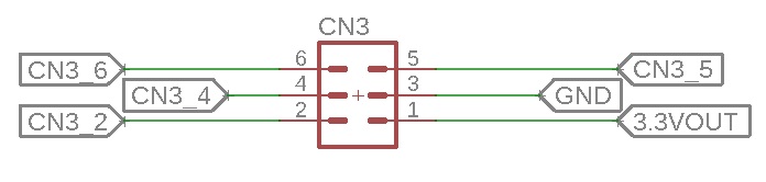
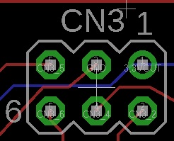
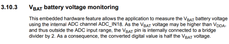
IMPORTANT NOTE ABOUT BATTERY VOLTAGE MONITORING (PG 19 OF STM32 DATASHEET):
RESOURCES
- Through Hole Package Design – http://www.msilverman.me/2010/06/creating-a-new-device-in-eagle/
- Use online trace width calculator in lecture slides to figure out trace widths
- According to Lecture 8 slides: https://engineering.purdue.edu/ece477/Course/Lectures/Slides/8-HardwareDesignTechniques.pdf
- General Signals – 8 – 16 mil traces (we use 12)
- Power bus – 24+ to 32 mil traces (we use 21)
Week 10
Date:
Friday, March 23, 2018
Total Hours:
8
Description of design efforts:
- Main PCB and Daughter PCB have arrived (x3)
| Part | Model | Supplier / # | Dimensions + Ratings | Price | Qty | Total | |
|---|---|---|---|---|---|---|---|
| 1 | Switch | Carling Technologies L11D1S001-AZZ00-000 | 432-1271-ND | 44.04mm x 22.02 mm; 12 VDC, 20 ADC | 9.27 | 3 | 27.81 |
| 2 | Terminal Block | Phoenix Contact 1729128 | 277-1247-ND | 1.3 mm hole diameter | 1.04 | 3 | 3.12 |
| 3 | PTC | Bel Fuse, Inc | 507-1769-1-ND | 2.5 A trip current | 0.125 | 10 | 1.25 |
| 4 | Inductor | Coilcraft | MSS6132-472ML_ | 4.7 uH, 2.5A supported | Free | 10 | 0 |
| 5 | RSNS | Panasonic ERJ-8BWFR024V | P.024AUCT-ND | 1206, 1W, 24m | 0.618 | 10 | 6.18 |
| 6 | Switching Regulator | RT7294AGJ6F | 1028-1458-1-ND | Listed above | 1.26 | 5 | 6.3 |
| 7 | LDO | STLQ015M33R | 497-15934-1-ND | Listed above | 0.77 | 5 | 3.85 |
| 8 | Fuel Gauge IC | DS2781E+ | DS2781E+-ND | Listed above | 9.29 | 5 | 46.45 |
| 9 | Microcontroller | STM32 | STM32F051R8T6 | Listed above | 1.9 | 10 | 19 |
| 10 | Resistor | R4 | 541-3306-1-ND | 500 ohm, M1206 | 3.92 | 3 | 11.76 |
| 11 | Capacitor | COUT1 | 1276-2728-1-ND | 22u, C1206 | 0.35 | 5 | 1.75 |
| 12 | Zener Diode | D1 | MMSZ5232B-TPMSCT-ND | 5.6V, SOD123, 500 mW, current is irrelevant | 0.203 | 10 | 2.03 |
Week 11
Date:
Friday, March 30, 2018
Total Hours:
12
Description of design efforts:
- General Procedure:
- Apply flux to the part. Don't be shy to add large amounts of it.
- Pick the part and make sure it is the right value by checking using DMM.
- Tin the solder tip - make sure it is shiny by applying solder to the tip and cleaning on copper.
- For surface mount components,
- Apply solder to one pad.
- Then hold the part over the pad using tweezers.
- While holding the part on the pad, reheat the soldered pad until the part is positioned.
- Then move the iron away and let the solder solidify.
- Finally add solder to the other pad.
- For through hole components,
- Insert the through hole component into the holes with the terminals sticking around the other side of the PCB.
- Twist the terminals so that the component is held in place.
- Apply solder to the hole.
- Cut the excess wire off.
- For ICs,
- Place the IC onto the pads and make sure that they are aligned.
- Use a magnifying glass to verify alignment if need be.
- Apply flux to all pins.
- Using a narrow soldering iron tip, apply solder over all pins - just spread it in one fluid motion.
- Because you applied enough flux, the solder will automatically cling to the copper pads and pins.
- Verify that the pins were not warped by tweeking them with tweezers.
- Check for shorts using the continuity feature of the DMM.
- After all components have been soldered on to the board, run it under water and use a brush to remove the flux from the parts.
- Use a can of compressed air to remove the water from the board.
- Important Notes:
- Leaded solder is easy to use, but is a health hazard, especially if you are soldering for long hours without a ventilator.
- Non leaded solder, which is what our lab has, is harder to use, but is safer.
- Turn the soldering iron to about 600 F - that is the right temperature to use with a thin soldering iron tip to make sure the solder does not accumulate and clings to the part by virtue of surface tension.
- Always use proper ventilation - long exposure to solder can cause sickness.
- Solder shorter, surface mount components first. This will make soldering taller, through hole components easier as they will not fall off.
- Remove excess solder using a solder wick.
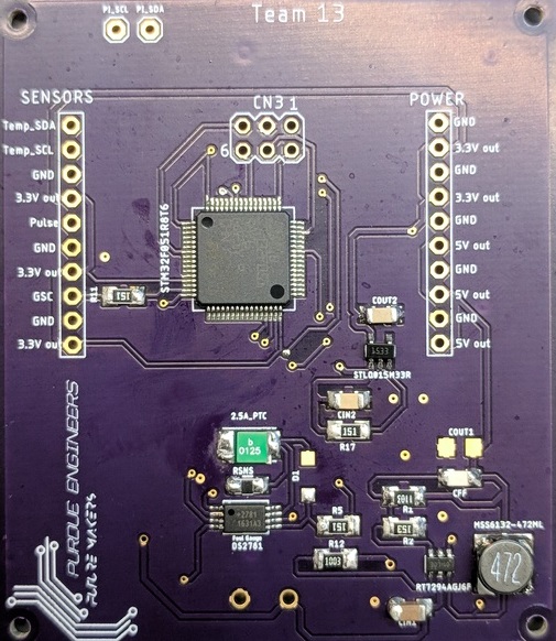
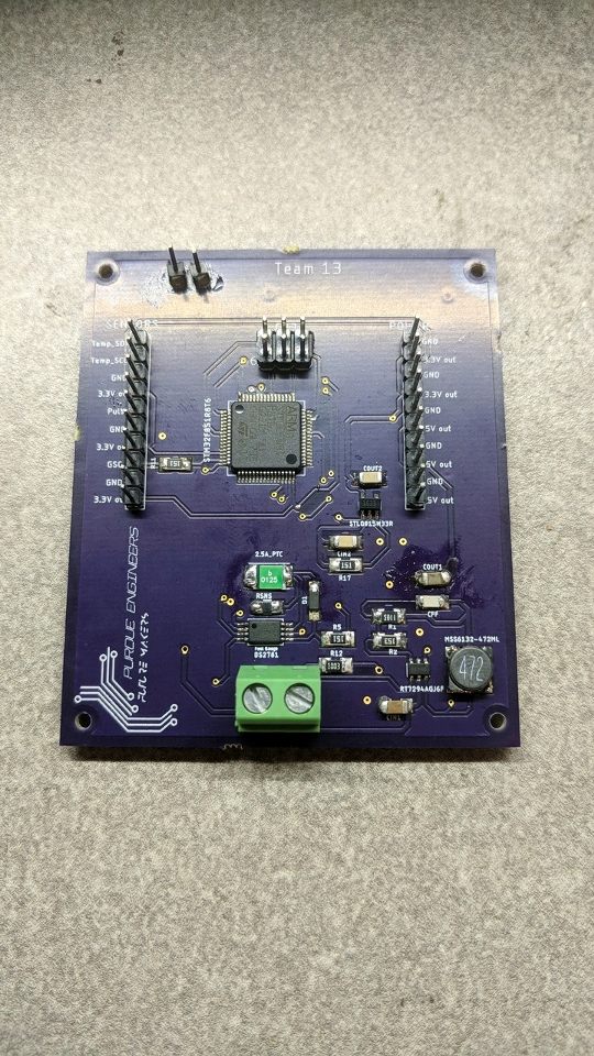
FRONT FACE OF PCB
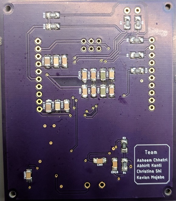
BACK FACE OF PCB
Week 12
Date:
Friday, April 6, 2018
Total Hours:
10
Description of design efforts:
- General Philosophy: Break the PCB down into different functional blocks.
- General Procedure:
- A good preliminary check is to ensure that the resistance between PWR and GND is of the order of a few kOhms
- Equipment needed:
- Power supply set to 7.4V.
- Ensure that current is limited to 150 mA. The reason this limit is chosen is that it is the current the narrowest trace in the PCB can allow. Therefore, it is the safe choice if in case there are any current leaks in the PCB.
- A DMM set to resistor mode with continuity function on.
- Point probes or banana cables.
- The next check would be to ensure that there are no shorts between components. Do this using the DMM to check the solder points.
- Finally, make sure the PCB traces are consistent with the schematic by probing points and checking for continuity.
- Issues:
- Diode D1 has not yet arrived
- 22 uF capacitor is not here yet
- Next steps:
- Testing will begin after all components on the PCB have been soldered.
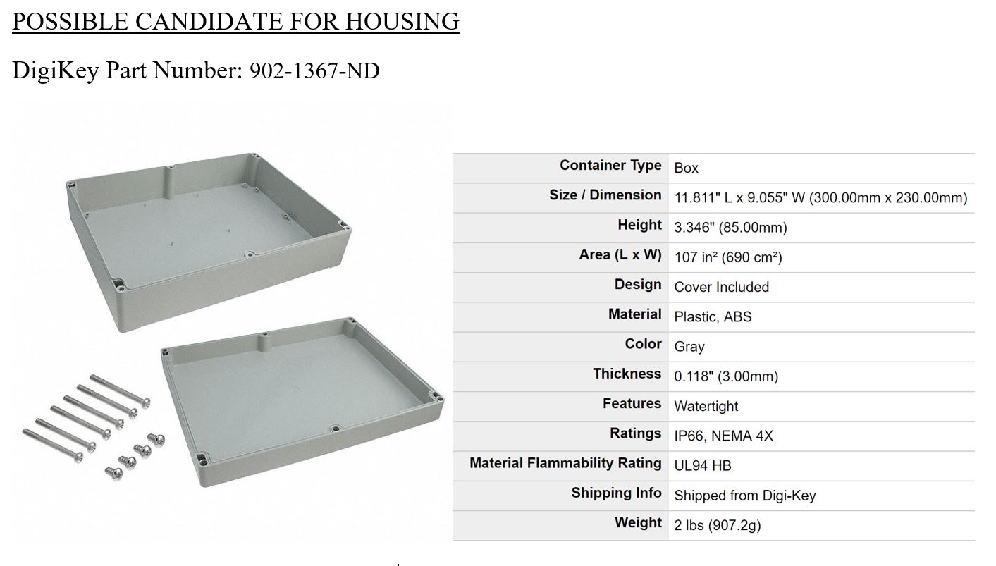
- Housing needs to be chosen.
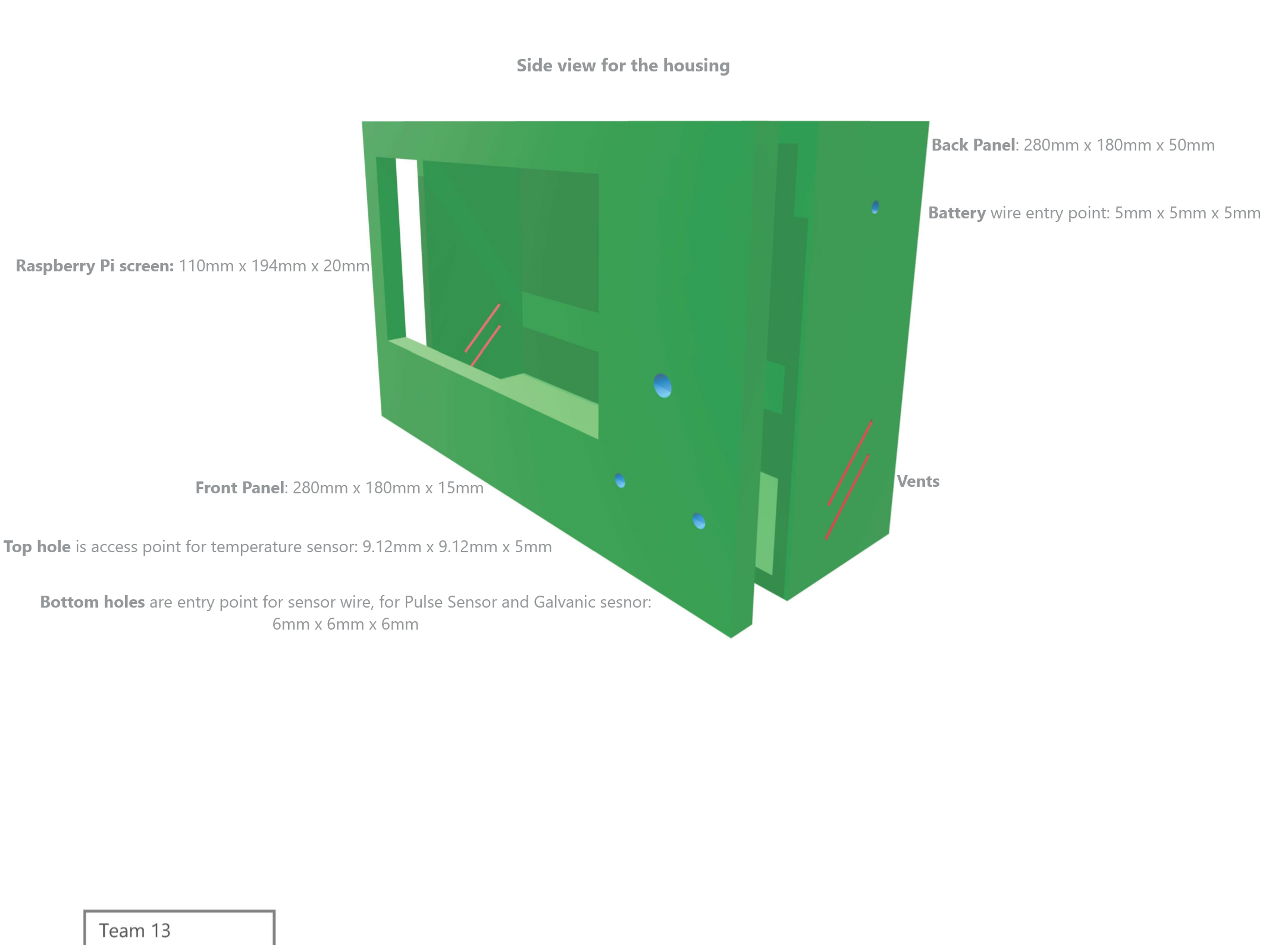
HOUSING PROTOTYPE DESIGN
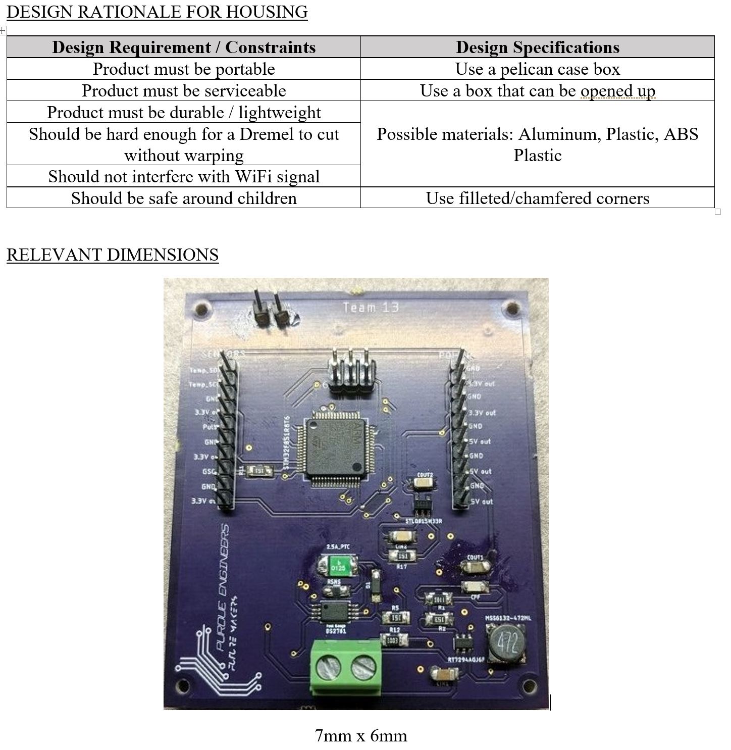
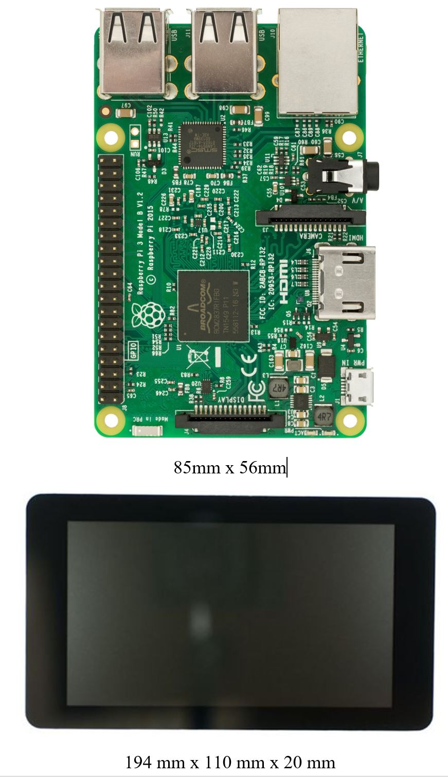
For housing of this type, a case from Digi Key will be ordered. I am choosing a Pelican case made out of ABS plastic. This will ensure that WiFi signal can get through while making it easy to cut out panels using a dremel. A pelican case with a lid will make maintenance easy while keeping the box aesthetically pleasing.
MORE UPDATES
PCB Soldering Complete
PRELIMINARY TESTING DONE
CHALLENGES FACED
Resolution: Use Diode feature of DMM and probe the two terminals. The terminal for which the positive probe indicates OL (Overload) is the Cathode.
Week 12
Date:
Friday, April 13, 2018
Total Hours:
10
Description of design efforts:

Week 13
Date:
Friday, April 20, 2018
Total Hours:
20
Description of design efforts:


Week 14
Date:
Friday, April 27, 2018
Total Hours:
10
Description of design efforts:
After this, I began building the housing. I drilled 0.093 in holes on 4 corners of the front face for the display and used a dremel to connect them. I used a similar technique for the power switch and ethernet ports. Finally, I added holes for the sensors and standoffs. Asheem improved the cuts by making them a lot cleaner - he created grooves to ensure that the sensors were flush with the front panel and made the cuts extremely clean and precise by using his strenght.