January 14, 2014 (2 hours):
Met after class to discuss preliminary project proposals. There were a few possibilities discussed. The end result was that a security system project was chosen. This project was enticing as it is very flexible (many different features can be added) and there is a real, viable market for this type of system.
January 15, 2014 (1.5 hours):
First manditory lab section. The main accomplishments was setup issues including creating user accounds, creating the team website, and so on.
January 16, 2013 (3 hours):
Met as a group with the primary goal of hammering out details for the preliminary project proposal. Heat, smoke, sound, and motion sensors were chosen to be included in the system. Personal responsibilities included Commercial Product Analysis.
WEEK 01 SUMMARY Accomplishments: Narrowed down design details. Set up user accounts for each team member. Submitted preliminary project proposal. Weekly Work Total: 6.5 hours Project Work Total: 6.5 hours
Week 02
January 22, 2014 (2 hours):
Started initial work on final project proposal. This included dividing up portions of the next assignment and assigning roles and responsibilities to each group member.
January 25, 2014 (5 hours):
This meeting originated as a time to finish the final project proposal. It was decided early in the meeting that the group was not happy with the current security system projects. Reasons for this include that: the project was too vague, there are far too many sensors that could be interfaced, and overall the team agreed that it was a generally uninteresting project.
The new project that was decided upon is at its core a hardware implementation of the
tone matrix web application.
January 26, 2014 (4 hours):
Met as a team in order to finish the final project proposal. See that homework for items such as design schedule, homework dates, homework tasks, and so on.
WEEK 02 SUMMARY Accomplishments: Changed project from security system to tone matrix device. Submitted final project proposal, project specific success criteria. Weekly Work Total: 9 hours Project Work Total: 13 hours
Week 03
January 29, 2014 (4 hours):
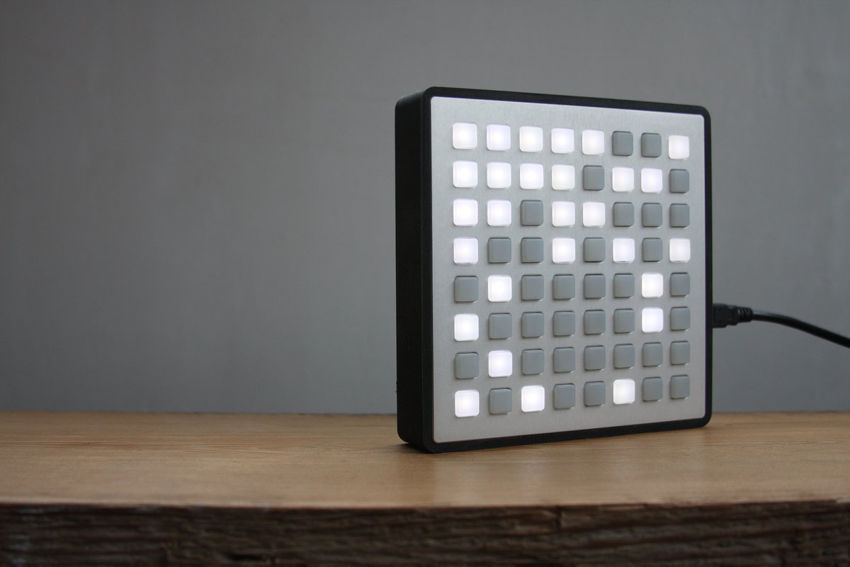
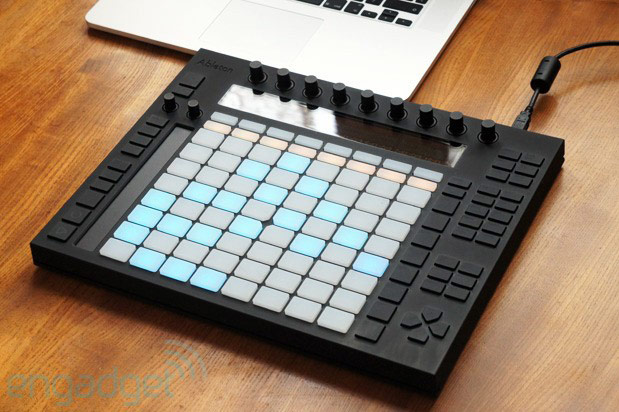
Met as a team to update HW0 with the new project details. Personal responsibilities include commercial product analysis. The three products that were detailed are as follows (click on picture for product website) Monome ,
Ableton Push , and
Novation Launchpad mini.
One commonality between these three commercial products is that they all must interface with a host device over usb. The BeatSquare will be a self contained product. There three devices also focus more on producing music rather than creation of music. See the report
here
for more information on these products.
January 30, 2014 (4 hours):
Worked on individual printed circuit board assignment. Other group members were present but the assignment was an individual one. The tutorial was meant to give an introduction to the program Eagle which will be used to make the pcb for this project.
WEEK 03 SUMMARY Accomplishments: Revised and re-submitted HW0. Submitted individual PCB tutorial assignment. Further developed success criteria. Weekly Work Total: 8 hours Project Work Total: 16 hours
Week 04
Feb 03, 2014 (3 hours):
The discussion on the 3rd included preliminary design constraints and parts needed in order to begin prototyping. Personal purchases include the tri-color leds from marlin p jones, membrane switches from sparkfun and corresponding sparkfun pcb breakouts.
Feb 05, 2014 (3 hours):
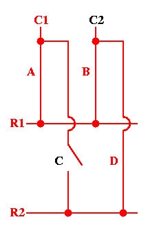
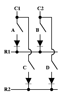
Met to further work on Design Constraint Analysis homework. Discussion of design constraints included: the hardware needed in order to interface with the LED's and buttons. The Sparkfun page for the breakout boards purchased on the 3rd contain useful information on scanning a button grid and eliminating ghosting and masking via the use of diodes (through holes for which are included on the purchased breakout board. Link
Here is an example of how diodes can be used to eliminate the ghosting and masking issues
The left picture will result in C incorrectly being registered as pressed whereas the right circuit will not because of the attached diodes.
Feb 06, 2014 (3 hours):
The main goal was to finish up the Design Constraint Analysis homework. See that document in the documents section for full Constraint analysis. Further discussion lead to the idea to remove the Rasperry Pi, webserver, and networked app portions of the project and replace them with the ability to save and restore to/from flash memory. This fits well with the overall project goal of a self contained device.
The microcontroller choice was narrorwed down to the Tiva C Series TM4C123GH6PM. This micro will fit the project well because it has a floating point unit, a good ammount of RAM and flash memory 32 KB and 256 KB respectively. This micro also includes relevent on chip peripherals such as pwm and QEI encoders. QEI encoders will be utilized for rotary encoders that will be used to adjust configuration parameters.
WEEK 04 SUMMARY Accomplishments: Completed design constraint homework. Went over parts needed in order to begin prototyping and software development. Purchased buttons, breakout boards, leds, and dacs to enable prototyping. Weekly Work Total:9 hours Project Work Total25: hours
Feb 11, 2014 (3 hours): Met as a team to work on the Product Packaging Homework assignment. Personal responsibilites include aiding the the commercial products sections. Personal responsibilites included the comercial products section . Products detailed include the Monome and Ableton Push. The Monome was chosen because of its particularly high end look, which utilizes custom milled wood exterior and anodized aluminum front.
The Ableton push was chosen as it is very similar to the BeatSquare component wise including an LCD display. See the report for more information on both of these product's packagings.
Feb 12, 2014 (5 hours): Individual work on notebook, commercial product analysis, explore launchpad tools.
Initial installation of the development suit Code Composer Studio on a laptop, however the installation proceedure conflicts with Mcafee security software so the installation forced to switch the installation process to another machine.
Installation proceeded on a personal desktop (with full administrative control of anti-virus software and firewalls). In order to download code composer studio one must register on the TI website (no official public download link available).
Link to the code composer page
Code Composer is based off of Eclipse which is open source. Code Composer does require a commercial (paid) license however there is also the option to evaluate for 90 days along with some other non-paid options that will likely fit the projects needs.
There is a power point presentation that goes over some code composer studio basics here: http://software-dl.ti.com/trainingTTO/trainingTTO_public_sw/GSW-Stellaris-LaunchPad/ppt.zip
Feb 14, 2014 (3 hours):
Helped to finish up packaging hw.
Recieved preliminary parts that where purchased. The Mouser order consists of three dip packaging DACs to be used for prototyping.
The chips ordered are 8, 10, and 12 bit DACS. The finial design will likely use a higher bit resolution but these will be useful for proof of concept type work and and will be allow a measure of prototyping and software development right away.
WEEK 05 SUMMARY Accomplishments: Aided in completion of product packaging homework. Ordered and recieved some preliminary parts that will be used for prototyping and will likely be used in the final product Weekly Work Total: 14 hours Project Work Total: 39 hours
Week 06
Feb 17, 2014 (1 hours):
More ordered parts came in these include the sparkfun LED/Button breakout boards and membrane switches.
With these components now in hand the team can now begin software development and proof of concept work.
Feb 18, 2014 (3 hours):
Began preliminary soldering on the sparkfun button pad breakout boards. Each of the 4 boards requires 16 LED's and 16 diodes (to eliminate button masking and ghosting). This means that there is a total of around 96 pads to solder.
A Eagle part library was also started. Preliminary parts were added to the library in order to facilitate PCB design in the future. A many of the integrated circuits that will be part of the BeatSquare do not have layouts in Eagle so custom layout will need to be constructed.
Feb 19, 2014 (2.5 hours):
Met in manditory lab. One suggestion from the course staff was to use LED drivers rather than sourcing and sinking all current from shift registers. The team will need to discuss this further (and perform testing) in order to decide which design will be used.
Feb 20, 2014 (3 hours):
Discussed the difference between using LED drivers vs shift registers. As the project will be utilizing persistance of vision there will only be a maximum of 8 LED's illuminated at one time the current needed to be sourced and sunk. Through testing it was determined that that the shift registers would be dealing with about 20 mA of current, within the operating parameters detailed in the datasheet. Furthermore more work was done on the schematic and theory of operation report.
Feb 21, 2014 (7 hours):
Finished up the theory of operation assignment. The assignment is available on the team website in the documents section.
WEEK 06 SUMMARY Accomplishments: Finished preliminary schematic, theory of operation, and hardware design. Further narrowed down hardware choices initial prototyping and parts ordering Weekly Work Total: 17 hours Project Work Total: 56 hours
Week 07
Feb 24, 2014 (4 hours):
Installation of prototyping software occured on the lab computer. The computer is running 64 bit Microsoft Windows 7.
This project will be utilizing a Tiva microcontroller. The evaluation board that will be utilized for prototyping this project is called the Stellaris EK-LM4F120XL Launchpad.
There is information about the product
here
Furthermore under the "Workshop Material" section there is a link to an
installation guide.
The guide goes over installation of drivers and the integrated development environment Code Composer Studio. As mentioned before code
composer studio is based off of eclipse so the interface is very similar. There are many examples available for the evaluation board.
The basic necessary procedure is to install Code Composer Studio then install StellarisWare. There was also a problem with a driver not being present and had to be downloaded from the source
here.
One of the more interesting examples is the floating point example in the
training workbook.
on page 171
This project will be able to utilize this hardware acceleration in order to possibly calculate sound output on the fly without need for a lookup table. This can further allow software features like custom waveforms and so on all without slowing the microcontroller down.
Feb 25, 2014 (5 hours):
Continued with examples on the Launchpad evaluation board. The lab computer will be utilized frequently to develop the schematic and PCB layout, so installation was replicated on a personal laptop. One helpfull example was the SSI example. A 595 shift register was interfaced with the Launchpad just as it will on the printed circuit board, however there were compilation errors that are not yet solved.
Feb 26, 2014 (5 hours):
Further worked on debugging the lauchpad SSI errors. The errors seem to originate from unrecognized pin names that should be defined in distributed header files. There is a helpfull article on the
TI support forums
Feb 27, 2014 (5 hours):
Solved the issue of SSI not operating correctly. The problem was that the header file pin_map.h did not have the proper definitions for the pins utilized for SSI. With these pins properly defined the SSI example worked as expected. One further neccissary modification was to put a wait call inside the shift out loop in order to be able to see the physical shifting otherwise the shifting happened so fast that all the LED's appeared to be on the whole time. A ammeter was place before the power in order to observe current. The recorded current was 42 mA however these are not the same LED's nor current limiting resistances that will be utilized for the final product so this is just a ballpark figure on what can be expected as far as current draw goes.
Feb 28, 2014 (6 hours):
Personally prototyped the selected power circuitry.
The following is an except from the LM317 regulator datasheet:
The component values are noted on that datasheet.
The constructed circuit:
The regulator was tested by inputing a 'noise' waveform from the function generator.
Here are the resulting waveforms. It can be seen that the noise was greatly reduced in the regulated output.
The red waveform is the regulated output the yellow is the noisy input.
The TPS37601 had some unexpected issues when initially prototyping. The part was expected to expected to be a 5v to 3.3v regulator however the incorect model was ordered and this chip is a 5v regulator instead.
As both parts were presently available it was decided to compare the performance of both circuits.
Here are the resulting waveforms. The Yellow is the noisy input signal green is the LM317 and red is the TPS73601.
It can be seen here that the LM317 performs much better at noise reduction than the TPS circuit.
WEEK 07 SUMMARY Accomplishments:
Installation of development tools for the evaluation board. Bugs were fixed that originated from incorrect header files. Example programs for the evaluation board were run including a floating point example and SSI example. Prototyped and tested power regulation circuitry.
Weekly Work Total:25 hours Project Work Total:82 hours
Week 08
Mar 2, 2014 (5 hours):
All the components for the LED pushbutton breakout boards have been soldered on, however there still seem to be problems with some of the boards. The problematic boards were tested and it was determined that the issues stemmed from having two different sets of LED's. One set of LED's (from MPJA) had a particular pinout (red, common cathode, green, blue) whereas the other set of LED's had a differing pinout (green, common cathode, blue, red). The problem with this is that the differing colors have different forward voltages. Thus the differing LED's with the lower forward voltage will turn on and sink all the current before the other LED's turn on. An attempt was made to desolder the problem LED's so that each row would at least have th esame LED's and thus function properly, however on one board a pad was damaged so one of the extra breakout boards will be used instead.
Mar 3, 2014 (4 hours):
Met as a team to practice the formal midterm design review.
Mar 4, 2014 (5 hours):
Prototyped the audio amplification circuit. The amplifier chosen is a
TI LM386 low voltage amplifier.
According to the data sheet the maximum voltage for the input signal is 0.4 volts. In reality this voltage is much too low to be practical especially for this product.
Here are some typical applications from the datasheet.
The test circuit constructed was the circuit with a gain of 20. This means that to amplify to 5 volts an input voltage of 0.25 was used. The resulting sound from this amplified waveform was very distorted and did not sound pleasant at all. An amplification from this low of a voltage will also amplify a lot of noise resulting in poor output waveforms. It was decided that a different amplification circuit would be needed in order to better suit the project's needs. As a replacement a
LM4902
was ordered. This amplifier circuit runs at 3.3 volts so no level translation will be needed when interfacing with the chosen DAC and micro controller.
Mar 5, 2014 (5 hours):
As TI somehow offers overnight shipping on free samples the new amplifier chip came in and is ready to be prototyped.
Typical application circuit:
This circuit was constructed in order to verify functionality. The circuit works well, the produced audio sounds much better than the low voltage amplifier as less noise is being amplified. Furthermore the gain can be adjusted or even set to unity.
Furthermore the LED breakout boards required more debugging. When certain LED's were illuminated others would turn on faintly.
Through probing with a multimeter and experimentation this was found to be a problem with leaving the other pins floating. When the other anode was connected to ground this problem was eliminated.
It seems likely that the problem here was some sort of inductive coupling that was forcing a current in the other line and the connection to ground solved this problem. This should not be an issue in the BeatSquared design as the shift registers driving these circuits would either be a logic high voltage or a logic low voltage never floating or high impedance state.
WEEK 08 SUMMARY Accomplishments: Prototyped amplification circuitry. Ordered new audio amplification IC and prototyped that chip as well. Debugged problems with LED breakout boards that included differing LED color pinouts and inductive coupling issues.
Weekly Work Total: 19 hours Project Work Total: 101 hours
Week 09
March 9, 2014 (5 hours):
The 3.3 volt power regulation circuitry was prototyped. The integrated circuit that will be used for regulation in the TPS73633
(datasheet available here)
There is an application circuit in the data sheet that details a recomended configuration that this project will be following.
Previously prototyping was done with the TPS73601 which is instead of a 5v to 3.3v regulator is a 5v to 5v regulator. Similar test inputs to previous tests were used to test this circuit as well.
The two values used for R1 and R2 are approximatly 9 and 5.5 kilo ohms.
Here are the results of testing the red line is the noisy input the yellow is the regulated output and the green is not used in this circuit.
March 12, 2014 (3 hours):
Met in mandatory lab. The course staff was generally pleased with the progress on the printed circuit board. One issue that the staff brought up was that the leads to each side of the optional crystal oscillator must be the same length in order to assure accurate clocking.
March 13, 2014 (4 hours):
The main focus today was proof of parts. This basically means that the custom PCB will be printed off to scale, then the parts that are already aquired will be placed onto the PCB printout. Any missing parts will then have a short writeup made detailing the part and so on. Also began prototyping the LED pushbutton array being driven by shift registers while the push buttons are active. There is not expected to be any ill effects with the two being active at once but it does not hurt to test.
WEEK 09 SUMMARY Accomplishments: Prototyped new 3.3v power regulation circuitry. Completed proof of parts. Started full prototype of LED pushbutton array.
Weekly Work Total:12 hours Project Work Total:113 hours
Week 10
WEEK 10 SUMMARY Accomplishments: Spring Break
Weekly Work Total:0 hours Project Work Total:113 hours
Week 11
March 25, 2014 (4 hours):
Assisted in developing the initialization routines for I2C. This comprised of reading through the manual on how I2C works on the Tiva development platform and on the DAC. One finding was that the DAC supports a mode where the address is sent once then the two data bytes may be sent , alternating, for an indefininte period. This means that the address could be sent to the DAC at initialization time then just the two data bits after that. This may allow for a greater effective speed of operation as the address will not need to be sent each time.
Firthermore the LED pushbutton matrix was tested with both the LED's and pushbuttons operational at the same time. The maximum current draw was observed to be around 300 mA.
March 26, 2014 (3 hours):
Met in manditory lab. The PCB has not arrived yet so available progress is rather limited. Prototyping with the
SN74HC165
parrallel-load shift register was done and operation was just as expected. The function generator was used to clock the shift register and every other data line was tied alternating to ground and power. An LED was used to observe the output.
March 27, 2014 (5 hours):
The custom printed circuit board arrived today. The power regulation circuitry is the first to be tested. Finished soldering the remaining power supply components. The capacitances used in the power regulation circuitry are slightly different than indicated on the schematic as the exact values were not available. The bulk bypass capacitor was increased from 22 uF to 33uF. This should not be a problem as this capacitance needs to be large not necessarily a specific value. The same turned out to be true for the noise reduction capacitance that was recommended to be 0.47 uF but instead a 1 uF capacitor was utilized for testing.
The power regulation was tested by using the same LED pushbutton matrix circuitry as previously used but with power supplied from the regulation circuitry rather than a test bench power supply.
A function generator was still utilized in order to provide the clocking signal. The clock rate could be adjusted to about any level, 1 Hz was used in order to readily observe the results. The first three rows of pushbuttons were used as inputs to the shift registers allowing for the testing of all colors.
One note on the colors: the primary colors (red, green, blue) all look good and for the most part uniform, teal (green and blue) looks decent with some uniformity issues and all the other mixes look fairly poor with significant variations in color throughout (especially noticeable with white). This project will likely only utilize the three primary colors but if the goal were to utilize all the colors some kind of regulation circuitry would need to be put in place in order to tune each cell's color.
It was decided to leave the white color on overnight in order to "burn in" or stress test the power regulation circuitry.
March 28, 2014 (0 hours):
The power regulation circuitry displayed no problems during or following the overnight test.
WEEK 11 SUMMARY Accomplishments: Prototyped LED pushbutton matrix both with desktop power supply and projects power regulation circuitry on the custom PCB. Assembled power regulation on PCB. Completed a burn in test of the power regulation circuitry.
Weekly Work Total:12 hours Project Work Total:125 hours
Week 12
April 1, 2014 (4 hours):
The evaluation board has been up and running and software development has begun on that platform however the microcontroller on the custom printed circuit board is in the end the final target and must also be interfaced with. The utilized programing hardware will be the Blackhawk XDS100v2.
Previously a hardware issue was noticed, wherein the pin sizes of the debugger and PCB do not match. The solution there was to create a transition board in order to match up the two different pin sizes and spacing.
This part operates using JTAG protocol for more information on JTAG see here. On the host side, USB is utilized to interface with the programmer. When utilizing Windows 7 no driver installation is neccessary. The connection however must be changed in code composer studio.
When attempting to first utilize the blackhawk debugger there was a linking issue where some symbols where re-defined. The problem was with headers that containted redundant information. The problem files where:startup_ccs.c and tm4c123gh6pm_startup_ccs.c. Eliminating one of them from the build solved the linking issues.
Simple LED-blink test code was used in order to assure that programing functionality was obtained. Helpful information on installation and use of this programer are located at the following sources:
http://processors.wiki.ti.com/index.php/XDS100#XDS100_Installation_Instructions
http://processors.wiki.ti.com/index.php/XDS100#Installation_for_Code_Composer_Studio_v5.1.x
http://processors.wiki.ti.com/index.php/Quick_Tips#Target_Setup
http://processors.wiki.ti.com/index.php/Quick_Tips#Target_Setup.C2.A0
http://software-dl.ti.com/dsps/dsps_public_sw/sdo_ccstudio/CCSv4/Demos/ccs4-setup1_b5.htm
http://processors.wiki.ti.com/index.php/Compiler_Installation_and_Selection
April 2, 2014 (3 hours):
Continued to populate the board with components. The methodology used when adding components to the board is to only add pieces one by one while testing for power stability in between. Power stability is tested by removing the power jumper (that will eventually be replaced by the power switch) then connecting a digital multimeter in order to observe current flow. An abnormal amount of current draw or excess heat observed on the regulation chips would indicate that there is a serious electrical problem that may result in damaged components.
One issue that was observed was that a decoupling capacitor was improperly routed so that it did not electrically conect from ground to the supply pin of the 74LVC8T245 level translator. This will likely not be a serious issue but may stress the power regulation circuitry and should be monitored.
April 3, 2014 (4 hours):
One minor problem was discovered on the PCB. The course staff recomended that the analog and digital grounds be connected at one point only, that point being the same point where the DC supply enters the circuit. On the PCB the analog and digital ground are connected at only one point, however that point is not near the ingress of the power supply. Fly wire-ing of the ground to this point may be possible, but the chosen course of action will be to test the circuit as is in order to see if this will be a problem or not.
Furthermore, a serious problem was found during population of the audio circuitry. After an amplification IC was connected the circuit was drawing over 800 milliamps of power, much more than is reasonable, furthermore the voltage regulation circuitry was far too hot for extended use. The board was investegated for shorts and probing with a voltmeter showed that the pad connecting analog ground to digital ground was registering at 3 volts meaning there is certainly an electrical problem. The exact details of which require more investigation.
WEEK 12 SUMMARY Accomplishments: Successful setup and programing of the Tiva microcontroller using the Blackhawk JTAG interface. Continued population of the board. Some minor, likely non-issue, problems discovered with the PCB. One major show stopping issue discovered, further investigation needed.
Weekly Work Total:11 hours Project Work Total:136 hours
Week 13
April 7, 2014 (4 hours):
The issue with the audio reproduction circuitry was determined to be an issue with the labeling of the pinout of the amplifier chip. The pins were incorrectly assigned when the custom part was constructed in Eagle. The result is that there is essentially a short from power to ground when the amplification chips are soldered onto the PCB. This issue can likely be solved by fly wire-ing the problem chips so that the correct pins may be connected to the correct pads.
April 9, 2014 (3 hours):
The course staff agreed that fly wire-ing the problem chips is a viable solution. Another solution suggested by the course staff is to bypass the amplification circuitry all together. This will likely result in a reduction in volume but this may be an acceptable, if non-optimal, solution.
April 10, 2014 (5 hours):
While a lookup table style approach to sine wave reproduction is pursued utilizing the built in floating point unit is investigated as well. The trade off's of using the floating point unit rather than a look up table include: less memory usage when using the floating point unit, possibly higher percentage of clock used, and possibly higher power utilization.
The floating point unit is straight forward to use. In order to use the floating point unit a few, built in, initialization functions must be called and then specific math functions must be used (ie sinf).
(Note that this example was previously tested on the evaluation board.)
One possible issue with using the floating point unit is as follows:
http://e2e.ti.com/support/microcontrollers/tiva_arm/f/908/t/274018.aspx
In short there may be situations where the compiler will generate non-floating point unit instructions even when the floating point specific function is used. The compiler developers likely wanted to maintain compatibility will many data types so that is likely why this design choice was made, however this also means that inspection of the assembly code most be done in order to assure that the floating point unit actually being utilized.
April 11, 2014 (4 hours):
After discussion about the method of sine wave reproduction it was determined that a lookup table style approach will likely be the best method. This project will almost certainly not be utilizing even close to all the available memory. Therefore the drawbacks of the lookup table approach are fairly negligible. Furthermore the results of the floating point units would then have to be quantized in order to match the data format of the DAC (which is just a fraction of the VDD not a floating point data structure).
Completed soldering of the fly-wired amplification circuitry. The newly wired circuit is stable electrically and testing will be done when software development is further along.
WEEK 13 SUMMARY Accomplishments: Determined and fixed electrical wiring issue in audio replication circuitry. Investigated usefullness of on chip floating point unit.
Weekly Work Total:16 hours Project Work Total:152 hours
Week 14
April 14, 2014 (5 hours):
One issue that must be solved is that the pinouts of the cables connecting to the 8x8 matrix array and the PCB have differing organizations. For example the 8x8 matrix is organized by rows and columns as seen here in Brennan's photo:
However the PCB is organized with headers for each color, the anodes, and the switches. One proposed solution to this was to create a translation board (using prototyping board) that routes all the wires to the desired locations, this however proved to be quite a bit of work so instead the solution was proposed that the cables just be routed individually. This leads to a rather unorganized look, however this will all be located within the packaging so the appearance is not a high priority issue.
Here is the result of routing the wires:
April 15, 2014 (5 hours):
Aided in development of software on the 8x8 LED button matrix. The PCB was designed with a slight issue where RCLK and SCLK are tied together whereas during prototyping these were separate signals. There is however the output enable signal that can be controlled and may be used to obtain similar functionality to the separate RCLK and SCLK. Another issue that arose is that when the use place his or her hands near the matrix it would often trigger a button press. It was determined that the cause of this was that the pull up resisters were not in this development circuit. They are however on the custom PCB so this issue should not be a problem.
April 16, 2014 (3 hours):
Started to aid in development of the audio reproduction software. There are many issues that need to be solved. Basic communication with the DAC does not seem to be reliably working, the current transmission speed is 333 kHz which is far too low for the audio reproduction. Development is hampered by a lack of documentation and the dificulty of debugging issues.
April 17, 2014 (3 hours):
It was determined that the digital oscilloscope in the lab has an I2C function that can display the data being output by the DAC, however it is difficult to see specifically what data is being output at a specific time.
WEEK 14 SUMMARY Accomplishments: Organized connections between 8x8 LED button matrix and PCB, aided with development of software on the 8x8 matrix and DAC.
Weekly Work Total:16 hours Project Work Total:168 hours
Week 15
April 21, 2014 (5 hours):
Further aided development of audio reproduction software. One big issue is that the DAC does not operate at the desired frequency. The documentation for adjusting the speed of communication is poor at best. As seen here the data sheet only mentions that "a specific command is used" with no mention of what that command is or how to use it.
i2cdataunclear
April 22, 2014 (6 hours):
With the now correct data set sine wave can be viewed on the oscilloscope. The frequency with which the data is shifting out results in a waveform that is far too low to be heard on the speakers available to us. After further investigation the function that determines the divisor for the I2C clock was isolated (also available here: https://github.com/vinodstanur/stellaris-launchpad/blob/master/driverlib/i2c.c). Of particular interest is the I2CMasterInitExpClk function. This function sets the registers for the I2C speed. As seen in this function there is a boolean argument that can be set in order to achieve "fast mode". Furthermore there are equations according to the documentation set the high speed mode clock, but no such effect has been observed.
April 23, 2014 (3 hours):
As seen in the previously mentioned I2CMasterInitExpClk function a clock divisor, ulTPR, was calculated. This divisor may also be independently set in order to obtain a desired I2C speed. In fact there seems to be no other way to change the I2C speed (beyond the "fast mode" set by passing in the "fast mode true" argument) other than setting this register.
April 24, 2014 (2 hours):
When attempting to output some notes on the DAC they will output once and then never again. One solution that was found to this problem is to explicitly send send multiple start conditions, which the DAC explicitly supports. Furthermore it was determined that the previously mentioned I2C speed selection divisor is in fact not a divisor at all but rather just a selection register, meaning that a "divider" of zero is the maximum "high speed mode" clocking rate.
April 25, 2014 (2.5 hours):
As a result of pervious work single and multiple tones can now be output to the speaker, however when attempting to output multiple tones the two tone data sets are added and then divided by two. The problem here is that the two notes are not specifically tuned so there is no good way to tell if the notes are just dissonant when combined or if there is another problem.
WEEK 15 SUMMARY Accomplishments:
Weekly Work Total:18.5 hours Project Work Total:186.5 hours
Week 16
April 28, 2014 (4 hours):
An attempt was made to tune the audio output by playing the note then attempting to match the note with the function generator connected to the same model speaker. The result is that the general frequency could be determined, however greater tuning accuracy is needed than we could achieve in this method.
April 29, 2014 (4 hours):
Audio was attempted to be ported to the main PCB. While single tone reproduction works as on the evaluation board, multi tone audio is similarly not working.
May 1, 2014 (6 hours):
Further issues were discovered with the audio reproduction software routines. In order to output sound a lot of cycles must be committed to these routines. This seems to be interfering with other functionalities such as the LCD and user controls. It was determined that multi tone audio reproduction was unlikely to be fully functional by the end of the semester. In hindsight this could have been solved by utilizing a dedicated audio processor, which could even be a microcontroller.
May 2, 2014 (2 hours):
Presented at the senior design showcase.
WEEK 16 SUMMARY Accomplishments: Multi tone audio, speed, and volume were all functional on the evaluation board, however the audio could not be tuned, and the audio reproduction libraries took so many clock cycles that other software routines were interfered with.
Weekly Work Total:16 hours Project Work Total:202.5 hours
 ,
,
 , and
, and


 The chips ordered are 8, 10, and 12 bit DACS. The finial design will likely use a higher bit resolution but these will be useful for proof of concept type work and and will be allow a measure of prototyping and software development right away.


