Michael (Duncan) Swartz's Lab Notebook
Week 01
January 9, 2013 (1 hour):
Met as a team after class to discuss preliminary project proposal as well at type out Homework0.
January 10, 2013 (2 hours):
Installed ssh packages for Cygwin in order to access group account, and followed the course webpage's
guidelines on setting up the website. Set up this notebook for future updates to the development of the project.
WEEK 01 SUMMARY
Accomplishments: Submitted preliminary project proposal (Homework0), set up website and notebook.
Weekly Work Total: 3 hours
Project Work Total: 3 hours
Week 02
January 15, 2013 (1 hours):
Met as a team to work out how to set up the website for this semester. Looked into using a free online template as well as how to implement it.
January 16, 2013 (2 hours):
Met as a team to review the TA and professors' responses to our preliminary project proposal from HW0. Started rethinking on how to "up the ante" on our
project as well as ensure that our project would be able to move forward regardless of if its most innovative component, the Leap Motion Device, did not arrive in time to be integrated successfully.
January 10, 2013 (3 hours):
Tom and I met to further discuss the full extent of our project and develop our PSSC's after Tom consulted with the professors about the features that should be
included to satisfy the design criteria. We researched the feasability of implementing Java on a microcontroller as well as the rough cost of our project, with the main funds going towards the Kinect/Leap Motion Device
and the monitor (TFT was suggested to us, though the benefits over LCD or LED are unknown). Suggestions were made to add an SD card slot (or equivalent) in order to load games to the microcontroller and thus allow more
memory to be devoted to each game, as well as to add a D-pad for recording high scores. When the rest of our team joined we decided on keeping the loadable game idea while scrapping the D-pad for hand gestures.
WEEK 02 SUMMARY
Accomplishments: Knowledge of implementing a successful website, re-evaluation of our project.
Weekly Work Total: 6 hours
Project Work Total: 9 hours
Week 03
January 21, 2013 (4 hours):
Developed the website that will be used and updated this semester as our design project advances. Spent a decent amount of time investigating creating a secure
html page that could only be accessed by our team. Within this page will be a notebook entry submission form that will bypass the need to use a local editor to edit these notebooks every time. Made the skeleton form and
a (fairly insecure) password system, but will work to implement the submission form before the end of the week.
January 22, 2013 (3 hours):
We met as a team to discuss our feedback from HW01, and determined that the general mindset of the professors and TA's was that our current idea was not as
appealing as we believed it would be. Therefore, we brainstormed and drew up a new "HW01" with a brand new project idea, centered around the idea of playing "Rock'em Sock'em Robots" using a Kinect and servo motors to
control the robots' movement. Forward and back movements as well as punching movements would be directly translated into the corresponding robot's movement, complete with sounds and lights. We as a team personally feel
that this is much more like what the advising team is looking for, and hope that they will agree with us on the idea when we present it in our powerpoint presentation tomorrow in class.
January 23, 2013 (2 hours):
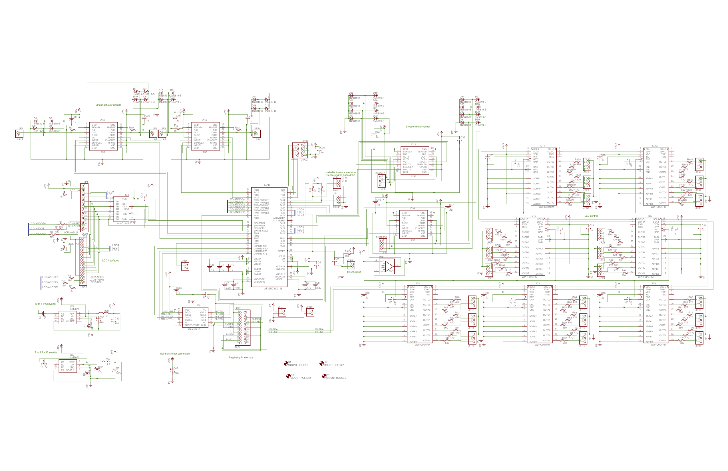
Started work on HW2 with understanding part design and pcb board layout with Eagle.
WEEK 03 SUMMARY
Accomplishments: Created the official website, brainstormed and developed a new project idea, started learning how to use Eagle to make our PCB schematic.
Weekly Work Total: 9 hours
Project Work Total: 15 hours
Week 04
January 27, 2013 (3 hours):
Met to work out the more specific details to our project, including a more accurate block diagram of parts needed, how the arena, kinect, and people will be
situated, as well as the sequence that the game will run at, from bootup unil the end of the battle.
January 28, 2013 (1 hour):
Finished work on HW2 (now that we know the proper parts to use). Created the schematic and routed the PCB as per the homework instructions.
January 29, 2013 (3 hours):
Met to determine the parts that would be needed for our project, to help Tom with his presentation of PSSC1 tomorrow morning as well as his completion of
HW3. Updated the website to our new project of Pop 'em Drop 'em Robots as well as deleted the "edit notebook" page and substituted with a links and downloads page.
WEEK 04 SUMMARY
Accomplishments: Specific block diagram details, part details, sequence of game operation.
Weekly Work Total: 7 hours
Project Work Total: 22 hours
Week 05
February 5, 2013 (4 hours):
Met as a team to aid Mark with his design of the packaging. Found a new power supply to use that could be found on digikey to make the part ordering easier.
Aided with a final analysis of all the parts we would need to complete out project, including factoring in how many extra parts to order in case we break components along the way, as we're likely to do. Lastly,
spent time figuring out the design on the power system. Looked though the datasheets to determine what components required external power supplies, as well as the voltages they would need, and compiled a list of
which buck converter chips would be used for what components.
WEEK 05 SUMMARY
Accomplishments: Aided packaging design and part ordering, started design on delivery of power to components.
Weekly Work Total: 4 hours
Project Work Total: 26 hours
Week 06
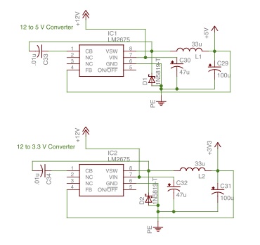
February 12, 2013 (6 hours):
Worked today on designing all the components needed to correctly use the buck converter chips (LM25576). I have come to realize that I overthought this by
a long shot; I had these chips ordered with the thought that it would be more convenient for outputting odd voltages to whatever source would need them. This would have been a good assumption, too, if we were not
simply dealing with 12V, 5V, and 3.3V components. I had found out a couple days ago that there exists simple linear regulators that convert input voltage to 5V and 3.3 V, and since we are using a regulated 12V power supply,
the LM25576's are overkill.
Regardless, I moved ahead and designed the entire dc-dc buck converter using the datasheet as well as design documents that Texas Instuments had placed on their product page to
help with design, since they suggest the use of 4 resistors, 7 capacitors, an inductor, and a diode. All this is meant to keep everything fail-proof in case of voltage or current spikes, prevent overheating,
maximize efficiency, and minimize voltage and current ripple.
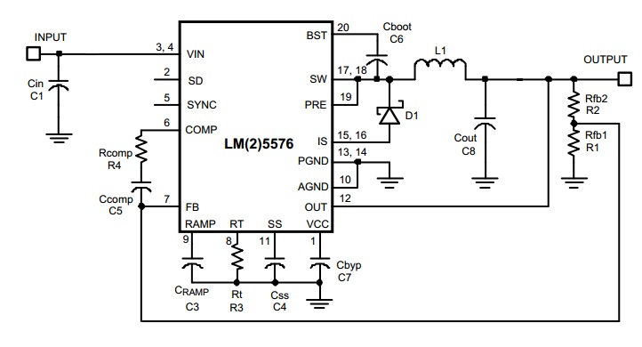
Luckily, I only had to design two converters; for 3.3V and 5V. For both, I
was also able to safely assume the reuse of all inductor and capacitor values, as they were all within tolerance range for such a small output voltage difference. The only difference was in the resistors near the output
that dictated what voltage was seen at the far side.
A majority of the time was actually spent looking up actual parts, and finding their relevant parts within Eagle so to make schematic design and PCB design
next week easier. The last obstacle is making sure the parts can actually be found over in EE. If not, then either I will have to order the parts IMMEDIATELY, find parts that work in EE and find or design Eagle
equivalents, or just scrap it all and go find these simple linear regulators, though I would hate to have those LM25576's (and my time spent tonight) go to waste.
February 13, 2013 (4 hours):
After presentations of TCSP's this morning, I went to the parts cabinet in the 477 room in the basement of EE, found most of the parts I needed (and the rest
of the part room on the first floor), and changed the package sizes of the parts that deviated a bit from what I had chosen last night. I also gathered enough electrolytic and ceramic capacitors to prototype the buck
converter on a board before first implementation on the PCB with the tiny surface-mount capacitors and resistors (size 1005 and 1206, respectively).
This evening I went ahead and made Eagle parts for
electrolytic capacitors that I will be using. It definitely refreshed my skills making parts, but after I had finished, I actually managed to find the EXACT part available under CPOL, which would make sense if my brain
was working properly.

Tomorrow I must go back to the EE parts room and find the two NEW inductor values I need, and figure out their case size so Tom can
complete the schematic, and I can make a correct PCB layout next week.
February 14, 2013 (1 hour):
I went to the EE parts room to see what inductor values were available, as I have determined that there is nothing wrong with choosing larger inductors than originally
calculated, because most all inductors will be able to avoid saturation mode since we will not be dealing with more than about 1.5 A through any part of the design. Also, higher inductance means less current ripple,
which is even more important in our 3.3V line, where we will only be drawing about 2 mA or so, which is obviously extremely small. I will have to prototype this extensively once parts arrive (hopefully) this week to ensure
my dc-dc converter does not have a larger current ripple than the current being drawn. If the ripple is larger, then the converter would enter discontinuous conduction mode (DCM), which messes up the voltage conversion.
Unfortunately, the parts room was out of the values that I needed, but I know now the package will involve vias, so I chose an Eagle part that would equal the larger size inductors to be safe.
WEEK 06 SUMMARY
Accomplishments: Designed the power supply system, calculated components values, found parts to use as well as their package size for Eagle.
Weekly Work Total: 11 hours
Project Work Total: 37 hours
Week 07
February 17, 2013 (4 hours):
Compiled a list of all notes that will be helpful for me with my design of the PCB board. I went through the documents on the course website, as well as Module 5,
on PCB design (very helpful). I need to check the schematic to ensure that their suggested components are on it, such as a bulk capacitor at the power input terminal and decoupling caps on each IC (I believe Tom did the
latter).
I also plan to go visit the TA's tomorrow morning to talk over my notes and clarify some details, including if some details of the PCB design are even necessary. For example, I don't believe the bulk cap
and ceramic cap are going to be of much help, because my buck converters are intricate enough that they should be able to remove the high-freq noise, and the bulk cap will be pointless for recharging the IC caps if the
converter simply regulates the cap discharge. In fact, this discharge could potentially throw off my output voltages, since they are set up for a specific input voltage. Perhaps the solution would be to put the bulk caps
at the power supply terminals AFTER the dc-dc conversion. To be determined tomorrow.
I also spent an hour giving our website a much-needed update. The gallery now has pictures, and the home page satirically
advertises our product to those that view our webpage.
February 18, 2013 (8 hours):
Went in the morning to discuss with Blaine some questions I had about the design of the PCB board from the info I had gathered yesterday. Cleared up a few
questions I had about copper filling for ground as well as separation of ground fills for digital, analog, as well as dc-dc conversion.
In the evening, I went to begin designing the PCB, but first
performed an Electrical Rule Check. Turns out Tom's schematic had over 150 errors as well as 200+ warnings! I spent the next 3 hours fixing these problems, which were generally wires that hadn't actually connected,
as well as fixing the types of pins of a couple of the manually-made parts to avoid errors when connected to passive parts, etc.
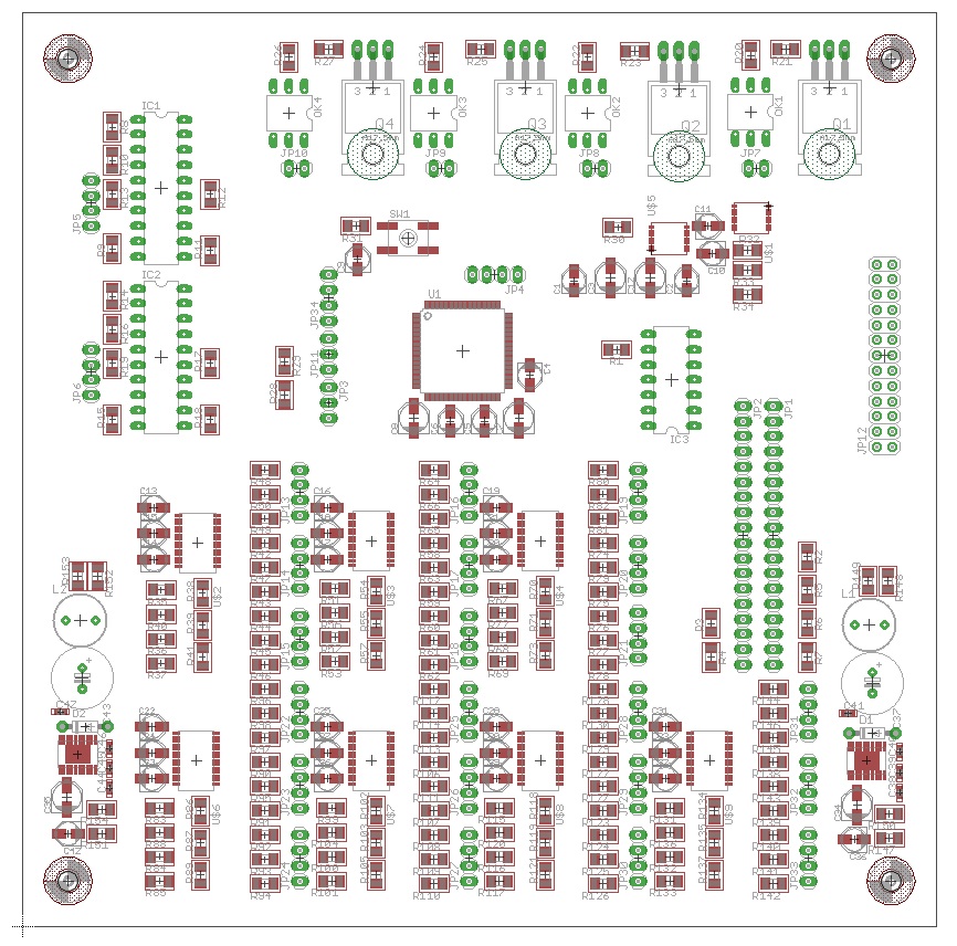
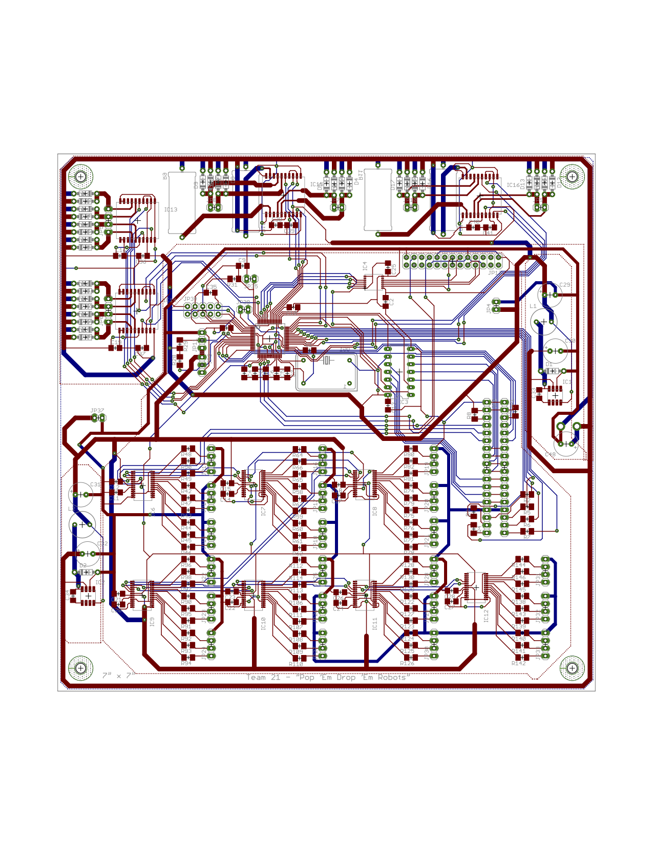
I realized we had over 300 parts to put on a board, as well at over 650 air
wires, which is a daunting task to fit on a manageable PCB. I chose a 6" x 6" PCB since it was advised by Blaine that larger wasn't likely necessary (though considering the parts sitting offboard were nearly a 6" by
6" square as it was without traces, this seems to be an exception). Regardless, I moved forward, adding small mounting holes on the corners, and set up the dc-dc converter systems on the edge of the board as best as
I could.
February 19, 2013 (11 hours):
Went to the lab in EE to continue work on the PCB in-between classes, because Eagle Light is stupid and won't allow me to place parts beyond about the 3" x 3"
area for some reason. I came to realize that the majority of the woes with my board had to do with the LED drivers. We chose to make our final project flashy, since it will have fun soundtracks playing as one
fights, and lots of tri-color LEDS seemed appropriate. The tradeoff was the need for 7 LED driver chips, each using 15 resistors and 3 large capacitors -- that's 133 parts right there! I spent a couple hours
determining the best way to squeeze these subsystems onto the board in a methodical, neat fashion, and finally came up with a shape that should work. I even managed to get each subsystem to be just over a 1" x 1"
square...this made the rest of my board much easier to work with (though I know the soldering of the parts here will be a monumental task of time, precision, and patience).
I finally managed to somewhat neatly get all the parts on the PCB, though there are undoubtedly going to be huge problems with getting the traces to where they should be among the LED drivers; I'll probably
have to be really smart about how I utilize the back panel to run traces. Beyond that, I spent a good amount of time creating my TSCP ppt for tomorrow morning (t-minus 4.5 hours); now time to nap for a few hours.
February 20, 2013 (14 hours):
The majority of today was spent tracing all 651 airwires on my PCB. What a monumental task. I worked in a 3-hour shift in the morning, a 2-hour shift after
class before dinner, and a 9-hour shift right after dinner. I managed to stay focused the entire time too, else I would have been a LOT farther behind. I knew I would spend the day Thursday studying for my evening exam, and
wouldn't be able to get back to the PCB until about 9 pm, so my goal was to leave a couple touch-ups to the PCB and the HW6 report for Thursday night.
Misson: ACCOMPLISHED
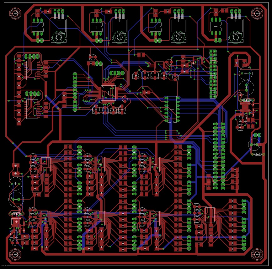
I know that we were told that it was better to start with laying power traces and ground, then run the other traces, but I had already set up general areas on the PCB for these traces. I was simply going to run
the traces to the outside of the board for power, and the ground was to be a rats' nest of traces throughout the board, since ground was needed EVERYWHERE. Plus, I had such limited space to work with that I
deemed it more logical to trace on a area-by-area basis. I started with the LED driver area, since it was the most cramped and in need of that initial freedom to trace anywhere. Then, I laid down the power and ground rails for
everything, followed by the jungle of traces for the microcontroller and other IC's on the upper-middle part of the board.
My main concern is that after running my power and ground traces around the board from their respective sources, many of the LED driver components didn't recognize these large traces as power or ground, and
instead insisted I trace between other LED driver components. This makes it quite difficult to see what is ground and what is power among the components, and don't like the thought of power being daisy-chained through
multiple nodes; luckily I'm fairly positive that even a fairly high EMI in the LED driver area will not be enough to affect how the IC and their traces operate.
One last thing I did last night (yes, long notebook entry, but also a long, long day) was to size up actual components to their package size from Eagle, as they FINALLY arrived Wednesday evening. About half of
them fit fine, but the microcontroller, L297, and MAX3391 were all the wrong size or pin style (DIP vs surface mount). So I had to get those fixed and the library updated, though I'm still experiencing a problem with one
part not connecting the pinouts to the package or something along those lines, and can't fix it. For some reason though, the part is correct in every way on the PCB so I won't worry about that this week.
February 21, 2013 (5 hours):
Today I didn't start working until about 8:30 pm, but thank goodness I did most everything last night. There wasn't too much to do except finish HW6, add a
couple parts to the PCB, and copper fill in the grounds for the dc-dc converter, analog, and digital sections. I presume I did it right, though it doesn't feel as such because now it's a bit difficult to see each
individual trace, but they're all there, just hard to see from the overview of the entire board. I guess it's to be expected when each trace is .01 inches and the board is 7 inches by 7 inches.
Final PCB after copper fill
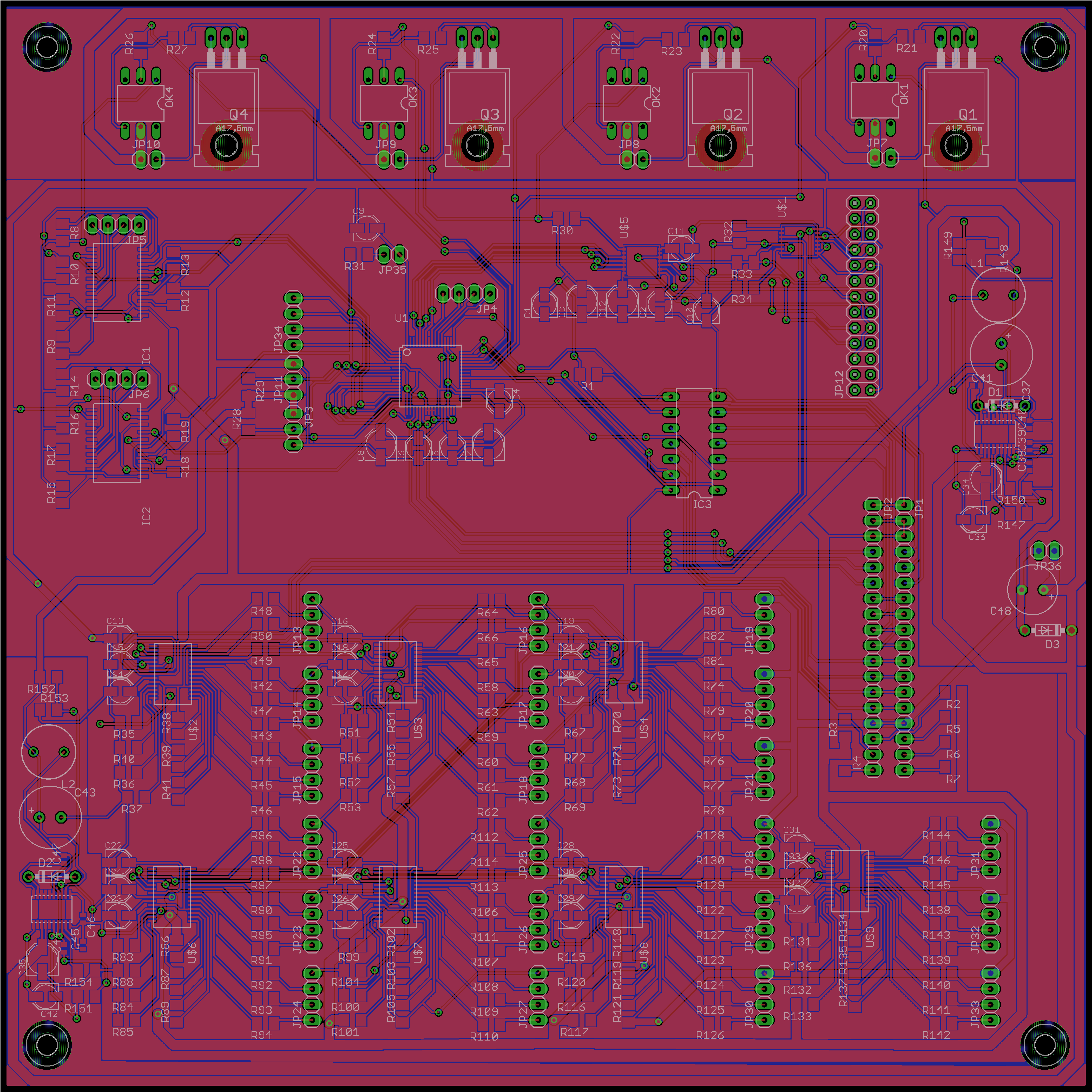
I added a large electrolytic capacitor from the power supply to ground as a bulk capacitor to power the decoupling capacitors for the IC's, as well as to suppress some of the voltage ripple from the power supply,
though it's not enough to (theoretically) affect my linear regulator systems.
WEEK 07 SUMMARY
Accomplishments: Created proper packages for parts on PCB, designed entire Printed Circuit Board, wrote up HW6.
Weekly Work Total: 42 hours
Project Work Total: 79 hours
Week 08
February 25, 2013 (3 hours):
Went to the lab to prototype the linear regulator system to ensure that we are getting 3.3V and 5V from the 12V power supply. Unfortunately the breakout boards
have the wrong pitch on them, so the pins don't match up. We also met as a team this evening to discuss what each of us will be talking about at our design review Friday, as well as discuss some changes that need to
be made. For example, we need different solenoids, and potentially they may be so large that we won't feasibly be able to do "dodges" anymore with stepper motors from the weight and bulk of the robot-solenoid systems.
Also, Tom informed me of the resistors on the LED drivers that could be removed related to the addresses, because they aren't needed. We also wired up all the IC's with resets to the single push button. It would have
been nice to know this early last week, since it would have saved me having to wire up over 60 components, and now I have to fix these open circuits where the part used to be, but I guess it couldn't be helped.
February 26, 2013 (4 hours):
Went to the lab after class to re-route the traces on the PCB where we removed all those components. It created almost 100 airewires to trace, but the general
infrastructure was there, so it wasn't too difficult. I had to delete the ground planes though so I could freely route the traces where they needed to go. I hope at the design review Friday the professors and TA's
won't tell me that the components are too closely-spaced together. I checked them on the 1:1 printout, and it seemed do-able, especially compared to having to solder the IC's with .5mm separation between pins.
We also met in the evening to discuss the future schedule of what we have to do for the rest of the semester to keep on schedule, as well as to work a bit on the design review powerpoint.
February 27, 2013 (4 hours):
Went to the lab to run a Design Rule Check (DRC) since I hadn't done that yet, unfortunately. There ended up being about 120 errors, though after fixing
everything that I could I found out about 65 errors were a result of the 3391 IC packages being made of all trace, where the square body should obviously have been on the tplace layer instead.
Tom went to the lab that evening with Mark to test the linear actuators we ordered to replace the solenoids that weren't powerful enough, and also worked on fixing the error we were getting with the
library not updating properly because of some error with the L297. It turned out that for some odd reason the package for the L297 was never properly saved or connected to the schematic symbol because the pins
hadn't been named the same when the package was redesigned from DIP (dual in-line packaging) to SMT (surface mount). After Tom addressed this issue and updated the library, he told me, to my horror, that the
package of the microcontroller, which I had spent so much careful time getting to be the correct size, had reverted to its old, wrong size! Seems that package hadn't saved properly either. That will have to be
addressed tomorrow, as well as fixing the traces that are now skewed on the L297, as the package Tom recreated isn't the exact same size as before.
February 28, 2013 (3 hours):
Went back to the lab to scramble to fix the new stuff that was messed up as a result of the library not updating. Luckily I still had a copy of the old
eagle files from Wednesday before Tom fixed the library, so I could used the "unsaved" microcontroller package to accurately and fairly quickly copy and finally save the correct microcontroller package.
I also fixed the traces, and ALL the DRC errors, now that the 3391 package was updated properly. I added a few decoupling caps to the power pins on the micro and IC's that had been overlooked earlier, and
also thickened the traced widths on all traces on the solenoid subsystem that dealt with the 12V voltage source, since they would all be dealing with the high current that the solenoids would be pulling. (Though
it looks now like we won't be using the solenoids in the end. For the design review tomorrow we will have to present what we have been working with so far. We don't have enough to change it officially just yet.)
Tom went to the lab to make the schematic look more readable in the evening, and made the unfortunate error of deleting wires on the schamatic when rehooking up to make cleaning up easier. Unfortunately,
he did not account for the fact that this also deletes traces on the PCB, so I had to help him through the process of rerouting these deleted traces, which was hard enough to learn in person the first time,
forget trying to explain over the phone. We eventually got it worked out, and I was able to use what we had finished with to make the PCB powerpoint slides for the presentation tomorrow.
March 2, 2013 (5 hours):
The design review yesterday revealed some relatively large changes that need to be made, and quickly, to our design. First and foremost, they recommended we
look at a simpler linear regulator than the 20-pin one I was using. To be fair, I had ignored the one they had us build earlier simply because I designed in case we needed to source the solenoids on 5V, and would
be drawing well over the 1 A maximum current that the linear regulator could have withstood. But now that the solenoids (or what we replace them with) will be sourced by 12V, we could revert to a much simpler design. So
I spent a couple hours researching a good mix of simple, accurate, and efficient linear regulators that had a relatively small footprint. For a while I looked at linear low dropout regulators (LDOs), which are
100% accurate, but they are also only as efficient as Vout / Vin, since the rest is disappated over resistors. I knew this would be bad because inefficiency would be as low as 30% and heat could rise quickly
over the resistors dropping down the voltage. So I finally settled on the LM2675Ms that we made in HW2 (yes, running full circle back to where we started).
I also researched H-bridges for controlling the linear actuators' push and pull, and perhaps with application for the stepper motors. I finally settled on a 8-pin SMT part that should fulfill all our needs.
I ordered free samples of the LM2675Ms for 3.3 V and 5.0V and ordered 8 h-bridges on Mouser, all rush shipping so we can prototype and show proof-of-parts to the TA's before Friday's PCB submission.
WEEK 08 SUMMARY
Accomplishments: Fixed the PCB for design review (multiple times!), researched and bought new parts for prototyping the recommended changes to our project for next week.
Weekly Work Total: 19 hours
Project Work Total: 98 hours
Week 09
March 5, 2013 (7 hours):
We met in our lab space to prototype what we could with our project and work on what we could before we show the TA's what we did Wednesday morning. I started
out by changing all the electrolytic surface mount capacitors that we had on the PCB from the Panasonic-B/C package types to 1206 surface mount caps as had been suggested during the design review. As I was doing
this, I also worked to change some of the other things on the PCB that were suggested to us. The first was moving the decoupling capacitors so they were as close to the power pins on the IC's as possible. This
proved to be a bit of a challenge since space around the microcontroller was quite tight from traces. So I spent considerable time moving the traces around in an orderly and DRC-appropriate way to accomodate
these changes, and actually think that I succeeded in making some older traces more efficient in terms of direct paths as well as trace use. It helped that we were able to eliminate a 3391 chip and that tangle of
traces from the board. I also rewired the LED drivers to be powered by 3.3V instead of 5V, mainly to make the 3.3V line pull more current and thus avoid current ripple that could potentially be larger than the current
being pulled by only the hall effect sensors.
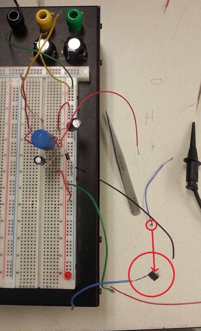
After this, I started work on prototyping the new LM2675 chips that we had gotten in the mail that morning. Unfortunately, we didn't inquire about getting breakout boards to accomodate the 1.27mm pitch of
this IC, so I had to try and solder 26-gauge wire directly to the pins. This took quite some time to get used to, but finally got it after about an hour. I hooked up the system, and after some fixing on connections,
got the 12V input to be converted to 4.97V, which is very close to the desired 5V! As if to curse me though, one of the pins broke off almost immediately after, and it was no longer possible to test, but I can now
say that the LM2675 will work just fine.
March 6, 2013 (2 hours):
This morning in lab we worked for the two hours until the TA's came around to check our progress. I spent the time implementing the new linear regulator subsystem
to our schematic and PCB. This involved creating the LM2675 symbol and package, wiring it up on the schematic, then tracing it properly on the PCB. Along the way I also modified the H-bridge package and symbol that
Mark made for me to work properly in Eagle. The end result looks much cleaner on our PCB than the old power conversion subsystem.
March 7, 2013 (11 hours):
Today we addressed all the final changes that needed to be made to the board, with the new linear actuators being the main focus. I spent time before dinner
working on cleaning up the traces that led from the micro, as well as changing the paths of the four resistors on the LCD screens to route to the micro instead of 5V. Mark had determined with George earlier in the day
that neither of them could figure out how to use the H-bridge IC's I had ordered last Saturday. Therefore, he had to find a new h-bridge and decided on the L298 IC that has been popular among other teams this semsester.
We could not test the IC since we obviously did not order it, and nobody else had one spare for us to borrow, so it was theory as we designed the subsystem and I updated it on the schematic and developed the package.
The development on the schematic and the placement and tracing on the PCB took most of the night. We had also determined that, unfortunately, the linear actuators would be pulling even MORE current than the old
solenoids, and would have to get a larger power supply, able to source 6A, to be safe. I hate having that much power going through the PCB, but I kept the power supply rails and analog ground isolated to the border of
the board to help with noise. I also don't like how thin the traces to the h-bridge were that would be sourcing almost 1A, but I made them as thick as possible for as much of it as possible to help alleviate heat, etc.
For this same reason, I added large packages for resistors meant to load almost 10W of power to ensure the linear actuators didn't pull too much current.
Then came adding the crystal oscillator that we had never added the first few times around. I added it to the back of the board since space for such a large part was running low, and the back will help prevent
corruption of such a sensitive signal. We also took the spare few pins on the micro and put them on another header. I belive that all but maybe one or two pins on the micro are wired to something now. After all that
tracing was finished, came the zipping of the appropriate files and submitting to www.freeDFM.com. It only took 4 tries to get it all correct, and the showstoppers that were coming back were simply trace spacing due to
the ground fill coming too close to the traces, which was an easy fix.
WEEK 09 SUMMARY
Accomplishments: Edited the cap types on the PCB, changed supply voltage on the LED drivers from 3.3V to 5V, redesigned the linear regulator system using a simpler model,updated on the schematic
and PCB and prototyped (badly), assisted design of the h-bridge/linear actuator subsystem, implemented on the schematic and PCB, finished up final PCB for submission to the fab house.
Weekly Work Total: 20 hours
Project Work Total: 118 hours
Week 10
WEEK 10 SUMMARY
Accomplishments: NONE; Spring Break in Ireland!
Weekly Work Total: 0 hours
Project Work Total: 118 hours
Week 11
March 19, 2013 (3 hours):
Met as a team in lab to work out different things that needed work on. Tom and Jackie worked on software while Mark worked on testing the L298 and linear regulators
properly with the breakout boards. I spent time trying to come up with a configuration to put the magnets on the robots' arms so that they can punch past each other to hit the opponent's chest without ther magnets
sticking to each other. They also have to be able to dodge while the arms are crossing. I found a combination where all the magnets sit on top of the fists, which keeps them out of the way since the arms point slightly
upwards while at rest. But they still tended to stick a bit. This will take some brainstorming. Next will be to find a way to mount the hall-effect sensors onto the robot's chest, as well as figure out the proximity of
the magnets to the sensor in order to detect a change in magnetic field that will result in a signal of a "hit" being sent to the micro.
March 21, 2013 (5 hours):
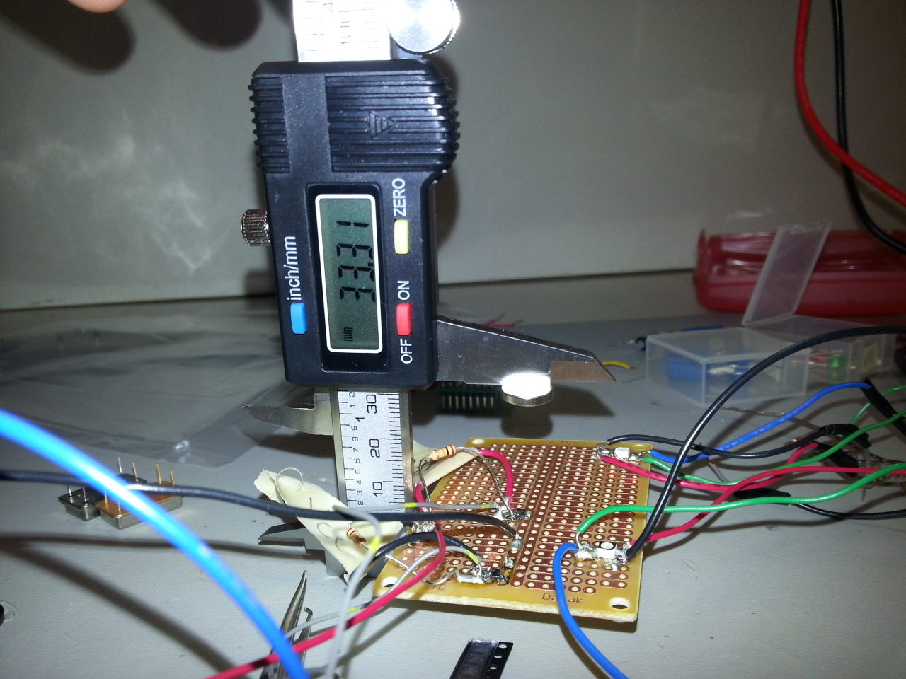
Met again in lab today to work on more things. Our PCB came in today, and looked great. I spent time trying to solder our hall-effect sensors to a board so we could
determine how far away the magnets have to be in order to trigger a change in the output of the sensor. After fiddling away for over 3 hours, I realized after borrowing Team 3's hall-effect sensor test board that the
chips we received weren't correct! Not only did ours read "800" on top instead od "L4A", but they were different sizes. I should have suspected something when I saw that our "sensors" had 5 pins instead of 3, but it looked
to be the right orientation of the pins, and figured the extra two were just no-connects.
Upon testing, I determined that our magnets registered a change at about a 32 mm distance (if you account for the magnet being inside the calipers), and didn't change back to the original high signal until much farther
away at around 50 mm. I realized that we could solve the magnet-sticking problem of yesterday by simply putting the magnets on the chest, and the sensors on the arms. Therefore, we can add some weaker magnets to the chest and get the
close "hits" that we desire. In fact, I would like to test those flat fridge magnets to see if they would be strong enough to work, and we could cover most the chest with one to get a higher likelihood of a correct hit on any part of the chest.
March 24, 2013 (4 hours):
Met again in lab today to work on whatever needed working on. I spent time trying to get the Maxim 3391 logic-level translator working properly. I wasn't entirely sure what I should have been
looking for, but Tom helped with that. According to him, the sending of power to the Raspberry Pi was working properly, but for some reason the power output was acting at 4.1V instead of the wanted 3.3V, and we aren't sure why. I assumed a bad
chip, and went to the other lab with the microscope and soldered a new IC to the breakout board. It was a learning experience, working with .65mm pitches, but in the end I figured it out. Unfortunately, it ended in the same 4.1V result, so that will
require more looking up on our part soon.
WEEK 11 SUMMARY
Accomplishments: Designed a way to properly trigger "hits" for fists hitting the chest with hall-effect sensors and magnets, prototyped the hall-effect sensor, attempted prototyping on Maxim 3391, learned to solder
under a microscope (accurately).
Weekly Work Total: 12 hours
Project Work Total: 130 hours
Week 12
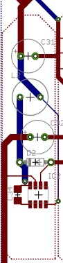
March 26, 2013 (2 hours):
Went to the lab to solder on the new inductors that I got from the parts shop upstairs as well as to fiddle with the 14 AWG wire Mark picked up earlier to fit in the power supply holes, since I made the
mistake of not making the vias large enough on the PCB. I ended up having to shear off some copper to get it into the hole, and to tin the wire I had to wrap some thin solder around the wire so it would flow through freely instead of bubbling and
getting "dirty" on only one side of the wire. Then I hooked the PCB up to the power supply, and after making sure it didn't blow up after a minute and measuring the 3 voltages that should be seen on the board, left for the day.
I went back the next day with Mark to make sure everything was looking okay, and after nearly 24 hours I can confirm the linear regular system is up and running fine with minimal heat (though that may change once the ICs and analog parts
start loading the regulator). The 5V line was reading ~4.98V, and the 3.3V line was reading ~3.28V, same as when I first hooked it up. I was getting the same value across the 12V lines as before at ~12.5V. I don't believe this should cause
any problems though since the 12V only powers the linear actuators, and the L298 chips can handle a much higher voltage than that. Besides, once the actuators start pulling current, then maybe the voltage will drop to ~12V, since the power supply
is only rated to output a certain wattage.
WEEK 12 SUMMARY
Accomplishments: Improved soldering skills, finished setup and burn-in of the linear actuators on the PCB, confirmed voltage outputs were within acceptable ranges.
Weekly Work Total: 2 hours
Project Work Total: 134 hours
Week 13
April 2, 2013 (7 hours):
Spent time working on my presentation for class tomorrow, TCSP #8 (Safety and Reliability Analysis). This was a very time-intensive presentation, since from looking at many of the old presentations
from past years, it seemed I had to do most all of my calculations and analyses for the presentation. Beyond that, they got rid of Microsoft Office on Software Remote, and I only use OpenOffice on my computer. This would normally be fine, except that
I know sometimes MS Office changes what is presented versus what I make in OpenOffice. Plus, making charts in OpenOffice was super-tedious, probably because I was doing something wrong. Whenever I made a graph, I had to change the color and visible
gridines for EACH square, and with a total of nearly 200 squares, this took a lot of time. But I still managed the time to calculate the Mean Time To Failure and error analyses for 4 components; the microcontroller, the L298, the linear regulators,
and the 1N5819 Schottky diodes (since there are 34 on our board).
April 4, 2013 (4 hours):
Today was spent finishing up Homework 11 on the safety and reliability analysis. Going through the calculations, it seemed to me that many of the numbers that were in the military handbook were
severely out of date. It is very impressive that a 35-year old book could still even be relevant to this day, when electronics have come so far, but at the same time, electronics have come VERY far. It seems that along the way, their safely and constant
failure rate would have gone down quite a bit. But, that's what we were given to go off of, and for our sake it is more than enough, since this is practice for industry more than actually intended for our use.
WEEK 13 SUMMARY
Accomplishments: Created TSCP #8, calculated the constant failure rate on four of our components, completed HW 11.
Weekly Work Total: 11 hours
Project Work Total: 145
Week 14
April 8, 2013 (5 hours):
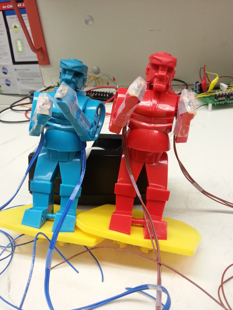
The majority of today's productivity was spent towards trying to figure out how to get the hall effect sensor subsystems installed on the robots' arms. It took a while to determine the best method, as the
circuit would have to fit on the fist so the N-S pole faces orthogonal to the body of the robot. That way, as the fist approaches the chest, the sensor will trigger a hit. It was found that the best way was simply to solder the hall-effect sensor and surface-
mount capacitor onto a small space on a piece of breadboard, and break it off into a small chunk about 1/4 square inches. It fit fairly well, and will look nicer once we replace the scotch tape with electrical tape. We can call them the robots' "boxing gloves".
The wires will have to hang loose by the robots' sides unfortunately, because trying to hide the wire by taping it to the body of the robot in any way impedes the ability of the robots to punch freely and for the arms to fall back down completely.
Also, I tested the linear regulators from our power supply, where they would be drawing as much current as they wanted to see what they actually pulled. Turns out that was about 5A! But, when we put our 10 ohm, 10W resistor in series with it, it reduced the
current to almost exactly 1A, which is exactly what we wanted. We tested the linear regulator's push on the punch pin of a robot and it had a lot of kick, so we can now confirm, after many weeks of stressing out over it, that we WILL have punching action, and can
prove it works.
April 9, 2013 (4 hours):
Today's mission was making more hardware components (as will likely be my goal for the rest of senior design). The first half was centered around making the LCD screen subsystems. Tom had been
programming to them for a little bit now, and requested the final skeleton system that will go onto our project so he had something a little less finnicky to work with than a breadboard with wires. Mark soldered 18 wires onto a female header and a perfboard, and I
spent a good deal of time connecting up the LCD and potentiometer to the perfboard so it looked alright. In order to fit aesthetically on the board, I had to make my own jumpers between the two sides of the perfboard so the entire LCD would fit on it without hanging
off a side. I figured this would make our job easier when it became time to make the LCD subsystem's enclusure.
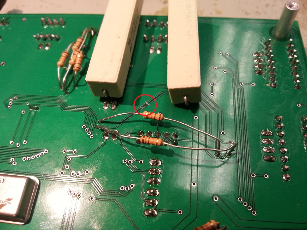
Tom also informed me that we had traced the tri-state enable to 5V instead of 3.3V, which we had determined to be correct at the time. So I had to take the PCB under a microscope to cut the trace for the tri-state enable pin and then flywire a connection to a
capacitor nearby that had 3.3V on one end. It took a while to get my relatively shaky hands to cut a .01-inch trace and then flywire to a .01-inch pin and pad, but the deed is done, though testing it is the only way to say for certain that the job was done correctly.
April 10, 2013 (2 hours):
Tom had gotten another couple perfboards, and today I went ahead and made the other LCD subsystem. Tom has to test it still, but I am confident it will work just fine. I used the same setup as last time with the jumpers
because I wanted the LCDs to be uniform in appearance. I get the feeling our project is going to look pretty shabby when it is all said and done, even if it does work, so whatever I can do to make it look more prefessional with minimal effort, I am going to do it.
April 11, 2013 (5 hours):
Today's lab session was not as productive for me as an individual, but was mostly spent helping Tom debug parts of the PCB. We went ahead and tested the L298s on the board, as Tom had not yet determined how to actually
use the micro to control the different pin outputs. It took some time, but he got it figured out, though in the process we determined that one of the micro's pins was fried, and we are wondering if it has to do with the L298 or if it was just a freak accident. Either way
that will need replacing (again).
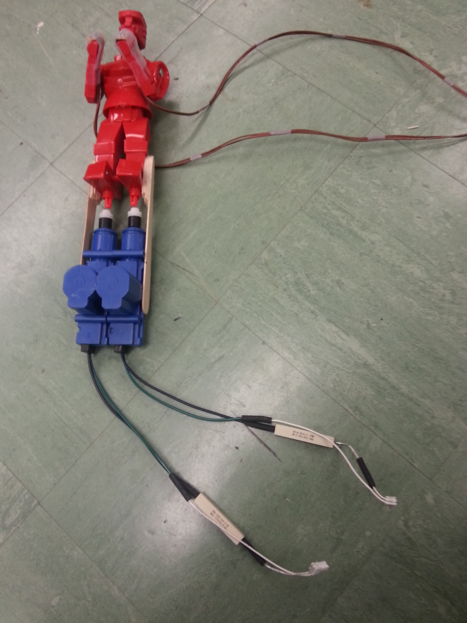
I also went ahead and attached the wires from the hall effect sensors of each robot arm to each other, and then to a 3 pin female connector that can connect to the appropriate headers on the PCB. Since the two arms' wires had to be in parallel, I solved the problem
of only one wire being able to attach to a pin on the connector by twisting the two wires together and soldering them so they wouldn't come apart. Luckily they were still thin enough twisted together to fit in the pin holes so I could solder them there permanantly.
WEEK 14 SUMMARY
Accomplishments: Confirmed the proper functionality of the linear actuators used for punching, made the hall-effect subsystem and attached to the robots, made the headers from the hall-effects to the PCB, made the LCD subsystems, flywired an incorrect
trace for the logic level translator, debugged ICs on the PCB and worked out the functionality of the L298.
Weekly Work Total: 16 hours
Project Work Total: 161 hours
Week 15
April 15, 2013 (3 hours):
Over the weekend, Tom informed me that while he and Mark were testing the linear actuators through the PCB, the just-replaced micro had fried, and they had determined that it was because we had been forgetful in our
last-second implementation of the L298 and linear actuator subsystem and forgotten optical isolators! When Tom went to the technician, Joe, and talked this over, Joe said adding a 10k resistor in series on these traces will solve the problem just the same, so that was today's task.
There were 16 traces I had to rip up, and I found it easiest to rip up a small section of trace between two closely located vias, then soldering the through-hole 11 kohm resistor (the lab was out of 10 kohm) to close the circuit. I tested all the connections, and they all read fine
without any shorts that would result in another fried micro, so it should finally be good to go when we test it tomorrow.
April 16, 2013 (5 hours):
Today was filled with more odd-end jobs that are slowly but steadily leading us toward this time next week when hopefully we will have our completed videos of the PSSCs and their success. It started with the simple job of taking a
dremel tool and cutting down the size of the LCD subsystems so they don't have all that extra perfboard sticking off one end. After that I took to Youtube to acquire our "battle music" that will be playing while users battle the robots. I found and edited clips to the Pokemon battle
theme, Sandstorm by Darude, Eye of the Tiger by Survivor and the Mortal Kombat theme song, and added them to the Raspberry Pi. I also completed the creation of several wires to headers for different components such as the speakers, linear actuators and stepper motors. Lastly I soldered
the other two L298s to the PCB under the microscope.
When we hooked up the linear actuators to the board to test them, we enountered yet again more problems. It seemed that there was only .5V going across the linear actuators, and a ~8V voltage drop afterwards between the negative end of the linear actuator and ground that wasn't
related to the power resister we added. Upon checking the L298 data sheet, we discovered that the power resister was put as the sensing resistor to help prevent current, but could only hold about 2V, so us putting the resistor there to act as a current limiter pulled too much voltage.
When we moved the resistor in series with the actuator, as we had thought it was on the board, it started working fine, though the resistor was getting quite hot. It's to be expected, but at least it didn't fry a 10W resistor
April 17, 2013 (2 hours):
We met in lab this morning for a progress check with the professors and TAs. They actually came by to our group relatively early, but I wasn't there because I spent the two hours making the revised wire setups of the robots, linear
actuators, and power resistors. I put one resistor in series with the blue wire, and then added white wire to the ends of both the resitor and green wire so they were the same length and crimped them to the white female headers. I then added heat shrink tubes to the open portions of the wire where I soldered the parts together
as a safety check to ensure we don't create any shorts from the free-hanging wires touching each other or parts of the board, especially since they will be carrying about 1 amp when the actuators fire. We were able to get one of our PSSCs checked off involving feeedback from a user that is displayed,
then shortly after I had left Tom and Mark got the robots punching through the PCB, though whether that was through a demo run in the micro or using the Wiimotes I am not sure yet. Either way, we have moved along quite nicely, and it seems that all we have to do now is to test the hall
effect sensors and hook it all up and make sure it works as one unit! We still have the PSSC videos to make, the instruction manual, and the final report to do (and Jackie is finishing up the poster), but those are trivial once our project is working on its own.
April 18, 2013 (3 hours):
Today is a turning point in which much of the remaining work on the actual project on my end is helping the others with their odds and ends, because hardware is practically done, and the packaging is Mark's department. The one last
thing I had to do today was ensure the hall effects were working. When we went to test them, a miracle occurred - two of the four were working! We had been told that they were very unreliable and that it wouldn't work, yet we had gotten them to. I spent time debugging the blue robot's hall
effect subsystems, and actually determined that the problem with one of the sensors was that a small strand of solder (no more than 5 mils wide) had connected ground and output voltage, causing the strange voltage at the output. Upon hooking it back up, we discovered that BOTH hall effects
on the blue robot had been bad, initially. On the second one, however, I could find no problems with shorts or open circuits anywhere. I resorted to completely changing out the hall effect sensor, upon which it started working immediately. I must have fried the old sensor when soldering, since
they are so small that a tiny blob of solder is enough to surround half the sensor with 700 degree Farenheit metal.
With this success, I used black electrical tape to hide the sensors tactfully on the fists and the magnets on the chest. It looks quite alright; we can say that the robots now have "boxing gloves" and a "chest pad"
WEEK 15 SUMMARY
Accomplishments: Fixed the high current problem on the trace from micro to the L298 inputs to prevent future micro failures, dremeled down the LCD subsystem, wired up different components to headers, found and edited our "battle music", troubleshooted the L298
and linear actuator subsystem, soldered the rest of the L298s to the PCB, completed the revised wiring of the robots/linear actuator subsystem, tested and confirmed the proper functionality of the hall-effect sensors as part of the whole system.
Weekly Work Total: 13 hours
Project Work Total: 174 hours
Week 16
April 22, 2013 (3 hours):
I came around to lab to mainly help where others needed aid, but most of the time was spent on software problems and waiting for glue to dry, so I wasn't an integral part of the work tonight until late when we began filming. We
took our box of blood, sweat, and tears over to the main lab room and I filmed Tom and Mark demonstrating the PSSCs of our project, and I spent the remainder of the evening editing the clips to make the video for our PSSC demo. It actually came together quite quickly and easily. I have
only an addition or two to make tomorrow, get the approval of the video from the rest of the team, and upload to Youtube to finish it.
April 23, 2013 (1 hours):
Today's task was fairly simple. I finished the end of the PSSC demo video and uploaded it to Youtube, ensuring that the song I added wouldn't cause the video to be pulled down for infringement issues. Luckily the song "Gonna Fly Now"
from the movie 'Rocky' is causing the video to only be blocked in Germany, so I should be okay.
April 27, 2013 (2 hours):
Today was the start to working on the final documents that need to be turned in Monday. Not much was done, but it was determined that it shouldn't be too bad the way we have the work divvied up currently.
April 28, 2013 (5 hours):
Today involved more work on the final documents and wrapping up the semester. It is actually taking longer than expected, namely because editing old homeworks up to par takes quite a while. I also said I would format HW 13 and 15 once
everyone had finished by transferring from Google Docs over to Word, which seems like it will be quite annoying as Docs messes up stuff quite a lot, especially charts. Hopefully it won't take long Monday, because I have a lot of studying to do for my Tuesdat morning final.
April 29, 2013 (3 hours):
Spent the entire time editing the User Manual and final paper (HW 13 and 15) from Google Docs to Microdoft Word, because Docs screws it up, and it needed to be a certain format. I was panicking a bit at the end because listing every
bullet point in the table of contents and linking the pages took a long time, but I got done and submitted on time -- but barely.
April 30, 2013 (1 hour):
The last task of Senior Design was finalizing the final presentation and making a couple touches to the demo video, then uploading the presentation and embedding the video on the home page. With that, I am all done with Senior Design,
and only the presentation in the morning stands in my way from freedom! Signing off for the last time, over and out.
WEEK 16 SUMMARY
Accomplishments: Recorded video of the successful PSSCs, compiled into our demo PSSC video, worked on, formatted, and submitted the final documents, embedded final video and uploaded final presentation. Finished Senior Design.
Weekly Work Total: 15 hours
Project Work Total:189 hours