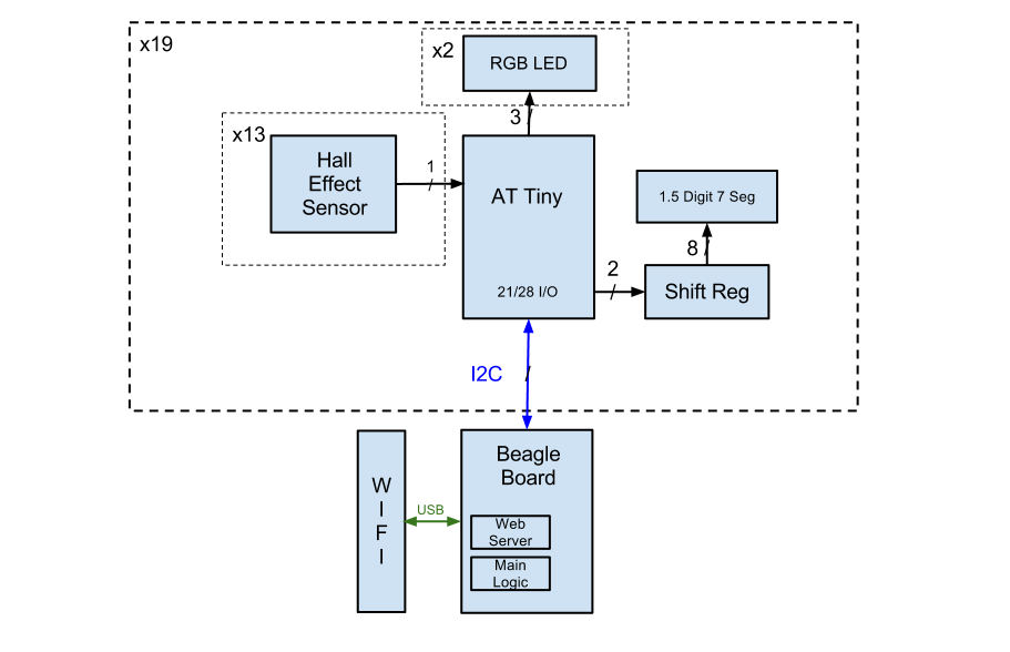
January 10, 2013 (3 hour): Met as a team to discuss preliminary project proposal. Team began considering necessary parts and costs. Ryan penned the proposal. Proposal was finished and submitted.
January 12, 2013 (4 hours): Met as a team to look into further details of parts needed. Ryan and Josh began work on the block diagram. Parts spreadsheet was completed. The team plans to order a few sample parts after speaking with the TAs in order to begin tinkering and interfacing with the AT Tinys.
WEEK 01 SUMMARY Accomplishments: Submitted preliminary project proposal. Created parts spreadsheet. Weekly Work Total: 7 hours Project Work Total: 7 hours
Week 02
January 14, 2013 (1 hour): Concerns about using 19 tiny microcontrollers arose. Went to office hours with Rob to discuss feedback with Blaine. The use of several micros and PCBs was discouraged. Borrowed a Beagle Board from Aditya. Discussed with Rob and researched options than using a micro for each hex.
January 17, 2013 (4.5 hours): Met as a team to discuss issues with the board construction and PCB size. Needed to formulate new plan of attack before writing the final proposal. Decided to move away from the multiple PCB approach by ordering a very large 18x22 PCB. This means we will forgo the multiple tiny microcontroller approach by installing several serial drivers for the 7 Segments and RGB LEDs. The Hall Effects can be sensed using a matrix approach to scan rows and columns. The matrix approach should work fine since our chosen hall effects have digital outputs. We selected a new main microcontroller which will handle piece sensing, display, and game logic, while the raspberry pi will be mainly in charge of the webserver. Ryan personally worked out the project proposal and search for new components. A new block diagram and part list had to be made as the design was completely recreated from the ground up. Will meet Monday to construct the presentation material.
WEEK 02 SUMMARY Accomplishments: Final Proposal completed, new design planned, several parts researched, presentation built for Wednesday. Weekly Work Total: 5.5 hours Project Work Total: 12.5 hours
Week 03
January 20, 2013 (2 hours): Began work with eagle to work on the tutorial. Met with team to update on status of parts and make the powerpoint presentation for Wednesday.
January 21, 2013 (4 hours): Continued to work with eagle and spent much time acclimating myself with the user interface and trying to find parts. There was much confusion on what parts to use due to conflicts in the assigment guidelines. Realized I would design many of them myself and decided to work on that later.
January 22, 2013 (2.5 hours): Worked with Josh to build a library of parts for the team to use for HW2.
January 23, 2013 (1 hours): Completed HW2 and left the documents for the team to turn in in my absence. Departing for San Diego tomorrow for an interview and won't be able to work with the new parts this weekend.
WEEK 03 SUMMARY Accomplishments: Finished the PCB HW and became familiarized with eagle. Presented the final proposal. Weekly Work Total: 9.5 hours Project Work Total: 22 hours
Week 04
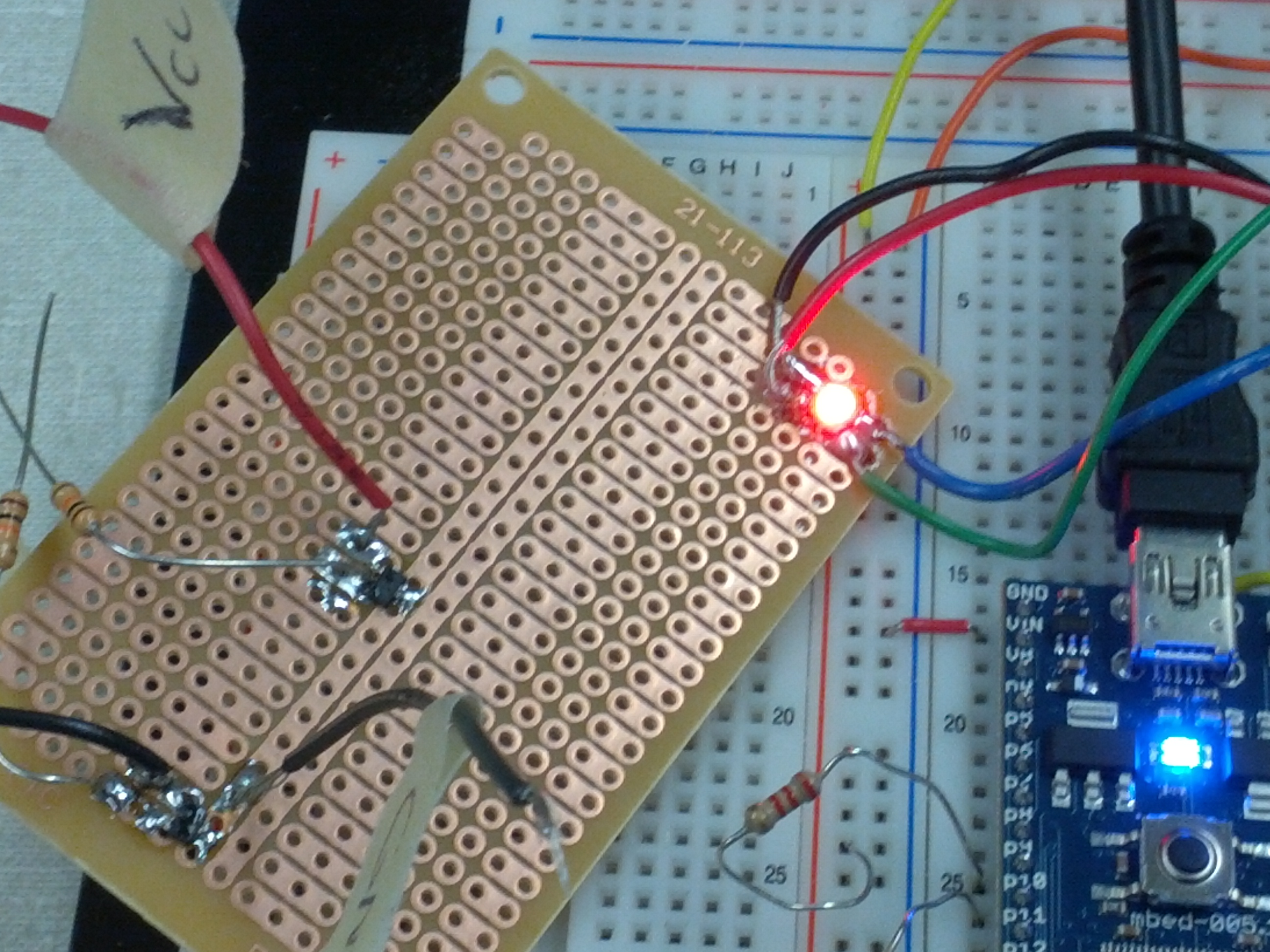
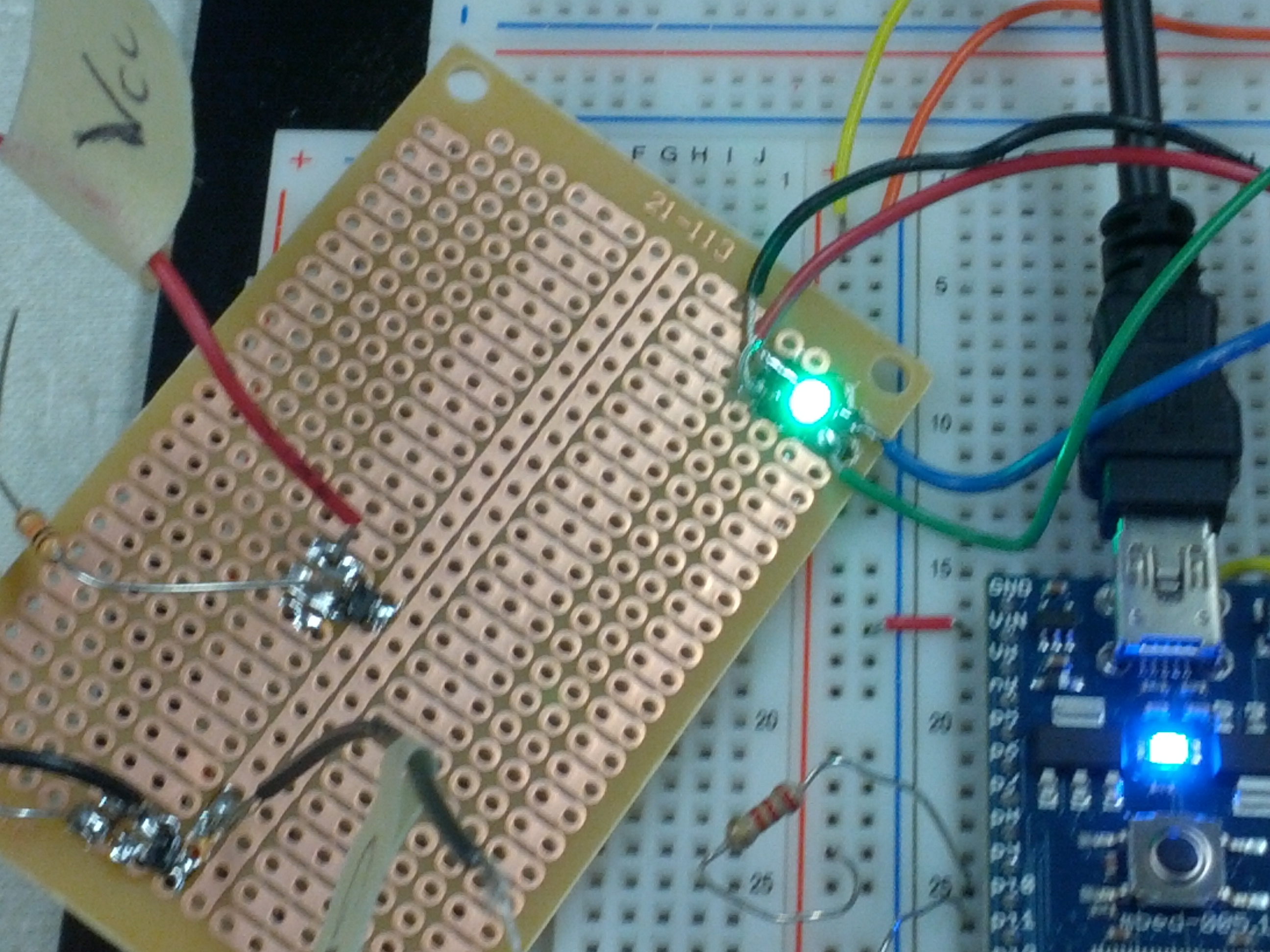
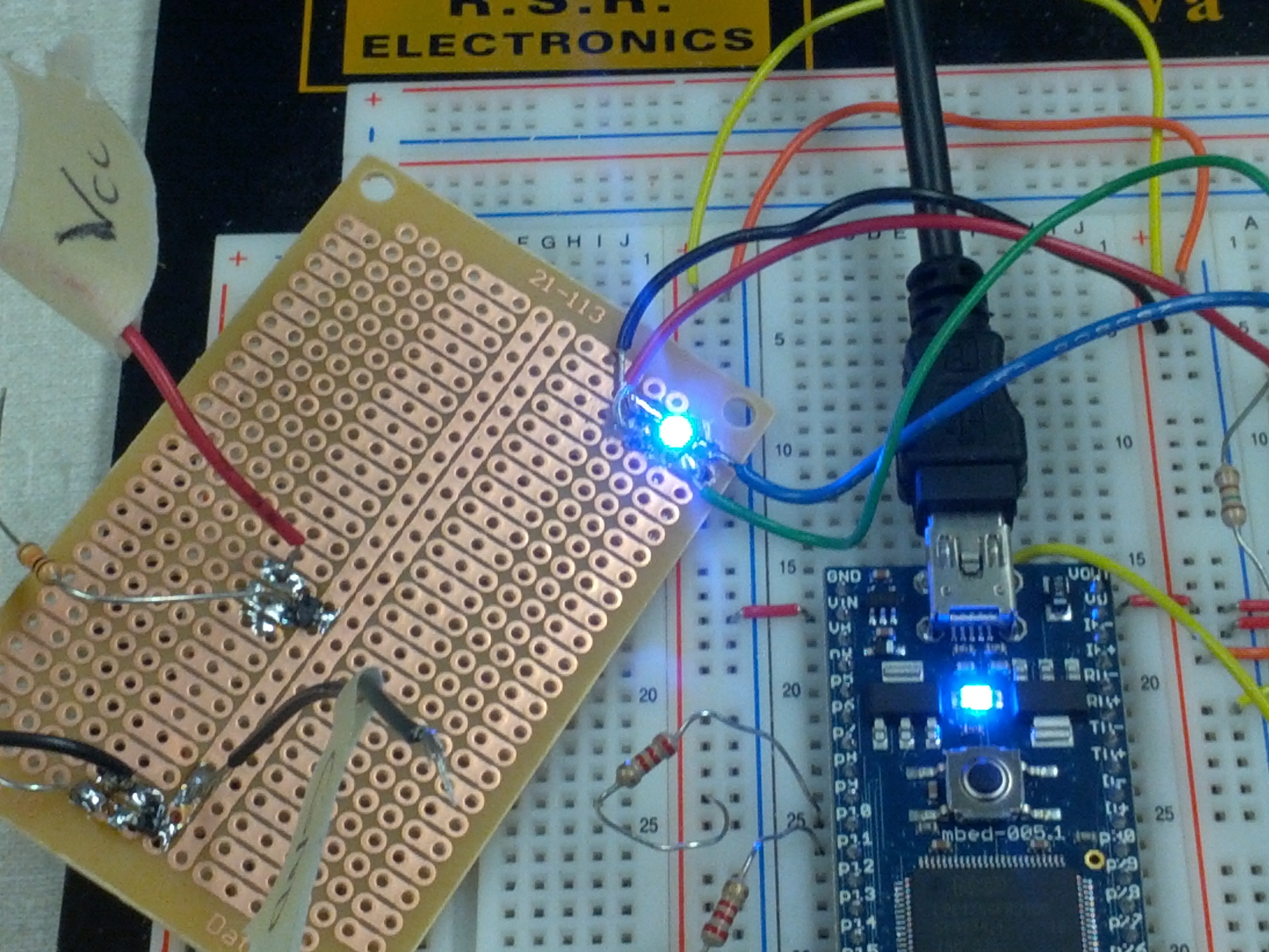
January 27, 2013 (5 hours): Met with Rob for a quick tutorial on how to program the test micro and his work so far on the RGB driver. Began trying to work out the problem with the I2C bus and why the 9-Channel LED Driver would not follow the commands and drive the RGB LEDs. I realized that the driver was deceptive in that is not controllable using I2C and a custom driver must be written to send commands. I spent a good amount of time writing a driver to cycle through the LED colors red, green then blue while testing the transition time and brightness settings. The LED looks sufficiently bright enough to diffuse through a small piece of frosted acrylic. The LED drivers can be cascaded and each RGB can be addressed easily on the same two pins. This will make it very easy to change the hex colors on the fly if we decide to give visual cues to the players this way.
January 28, 2013 (4 hours): Acquired three breakout boards from Aditya for the 7-Seg Drivers. After soldering one, realized the voltage requirement VIL of the drivers was very inconvinient when paired with our microcontroller of choice. Explored other options with Rob and selected and ordered a new driver to test with the board. Looking forward to working with the our micro and writting some drivers for increased usability of the RGB and 7 Seg drivers. I will be leaving Wednesday for another onsite interview after the TCSP.
January 29, 2013 (3 hours): Met with team to map out some of the design constrainsts to help Rob get a start on his assignment.
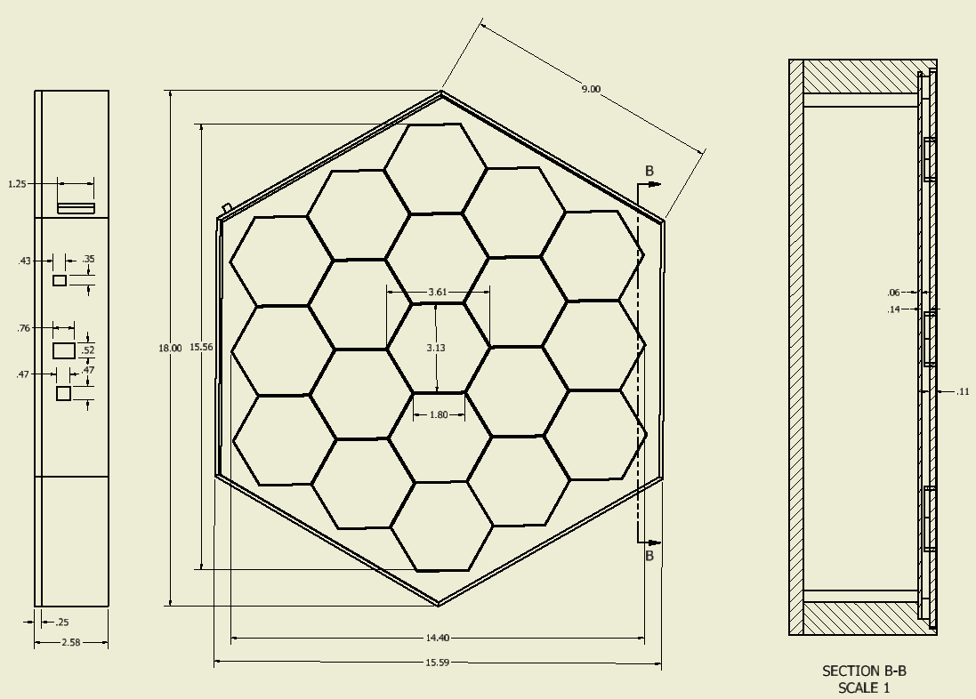
February 2, 2013 (4 hours): Began work on the CAD drawings. Tried out using Google
SketchUp, AutoCad, and Inventor. Felt most comfortable using Inventor and started work with that.
February 3, 2013 (6 hours): Continued work on CAD
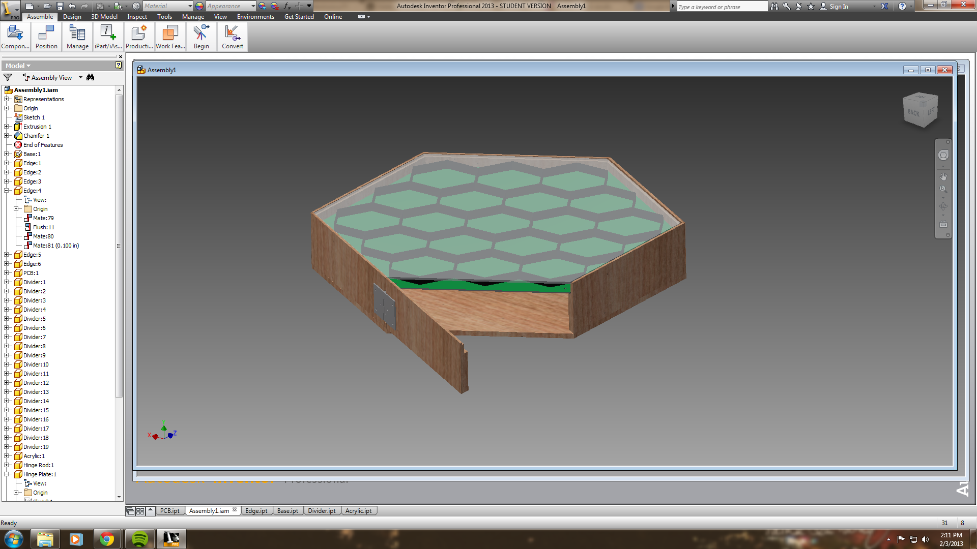
Design. Designed a two level board. The bottom contains the Raspberry Pi, Power Supply, and piece storage.
The top level contains a shelf for the PCB. A grid of plastic divders will separate each hex region on the PCB.
A plastic acrylic cover will sit about 8 mm above the pcb to leave room for the seven segments.
Started work on report. Found two comparable commercial products:
Dungeons and Dragons Computer Labryrinth
and The Generals. As a whole, finding board
games that implement piece detection and a board lit by LEDs is difficult and had to settle
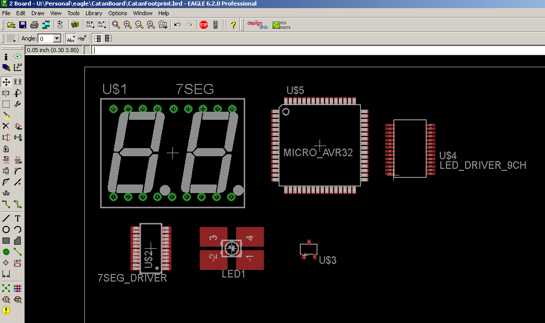
for these partially comparable choices. Started work on the PCB footprint.
WEEK 04 SUMMARY Accomplishments: Selected new 7 Segment Driver, built a set of constraints for the project,
completed most of the CAD drawings for the packaging and the PCB footprint. Designed footprints and schematics
for all major parts in the design. Weekly Work Total: 17 hours Project Work Total: 39 hours
Week 05
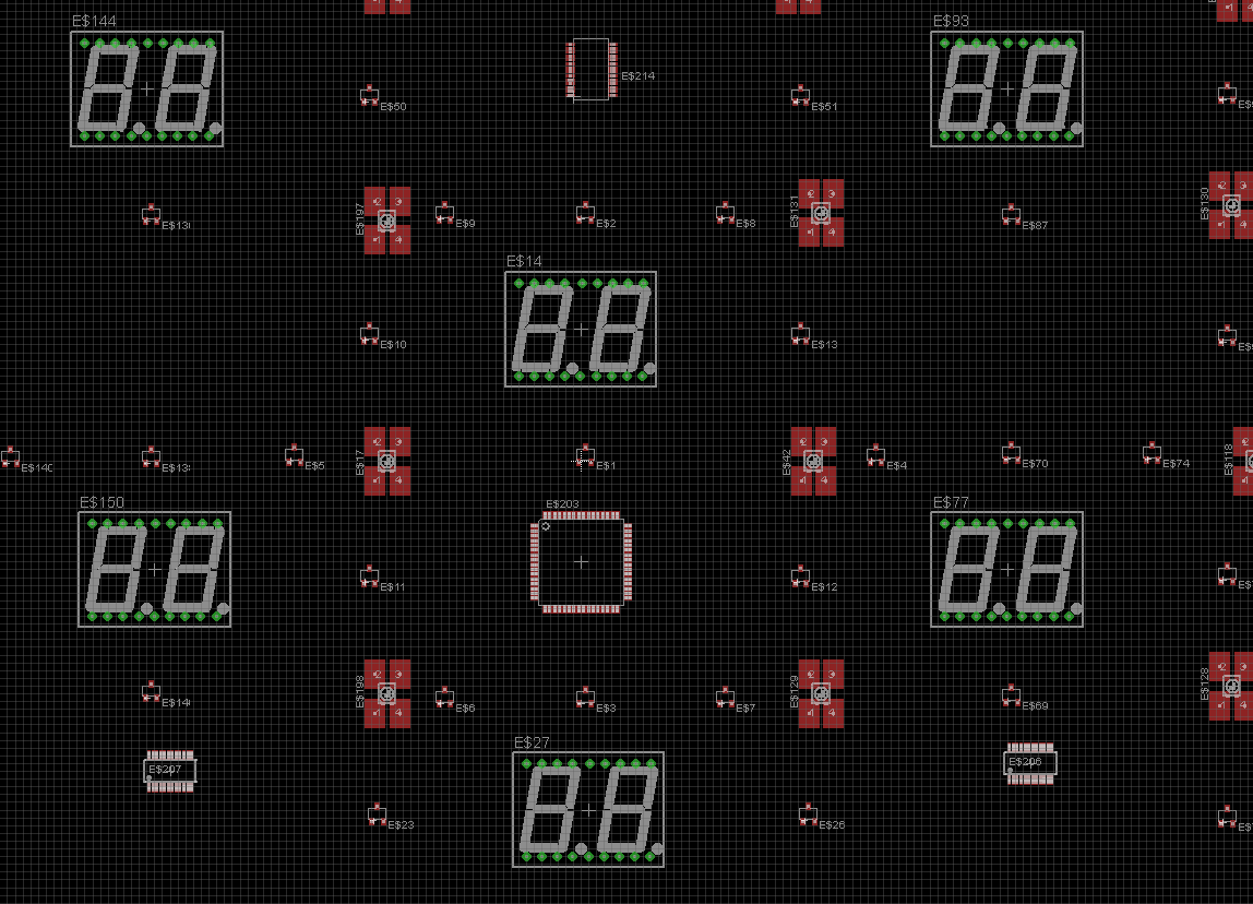
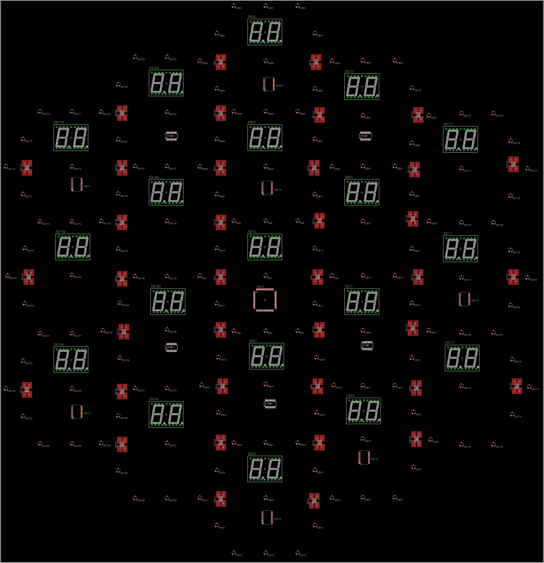
February 4, 2013 (5 hours): Continued work on the PCB Footprint. Finished laying out a preliminary footprint to estimate
the size of the PCB. It will need to be a size of about 18 x 16 inches. In order for the PCB to fit into our desired board shape, it must
be cut into a hexagon shape.
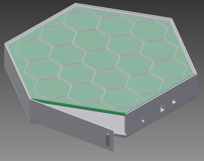
February 5, 2013 (4 hours): Met with team to complete the presentation for Wednesday and for feedback on the CAD design.
Found our major constraints to the packaging to be: a large flat playing surface, short distance between PCB and playing surface, semi-transparent
playing surface, opaque dividers between resources tiles, and additional space under the main playing surface. Realized we wanted to make the exterior of the package
from acrylic, not wood. Also decided to change the divider colors to white in order to reflect LED light. After meeting, I made changes to the design including
external holes for a power supply, rocker switch, and reset button on the side of the package. The features I had in mind to accomplish this were:
Rocker Switch and
Push Button. The micro has enough extra I/O pins to play with that we should be able to add these.
The CAD drawings and dimensions were finished and ready for the presentation on Wednesday.
February 6, 2013 (3 hours): Finished the write-up for the packaging report.
WEEK 05 SUMMARY Accomplishments: Finished the packaging report, finished CAD drawings, presented on the packaging design and completed a preliminary PCB footprint. Weekly Work Total: 12 Project Work Total: 51
Week 06
February 10, 2013 (5 hours): Worked with Josh to fix the RGB circuit. The issue was a simple misplaced wire. The driver sinks, not sources current. Ready to try out the circuit with the AVR Dragon when it broke due to a common issue where the power on the USB port dips too low. Examined documentation, related problems, tried to debug the Dragon, and flywire a fix with no success. We may have to order a new dragon or propose to use a different micro entirely.
February 11, 2013 (5 hours): Discussed with Josh and Rob about various options regarding the slain dragon.
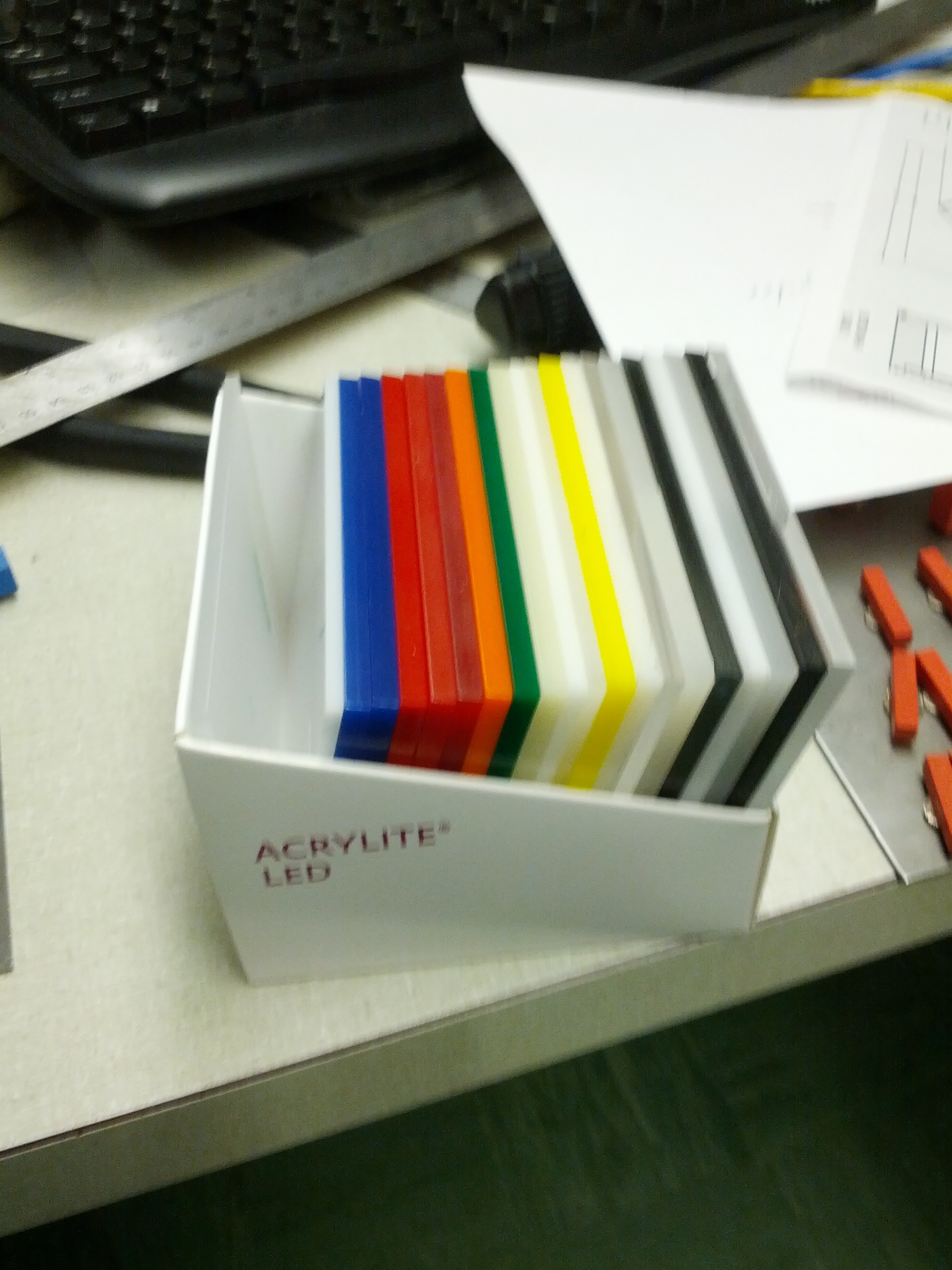
Decided to remain with the Atmel for now. Frosted Acrylic samples arrived to test. We were not impressed with the amount of
diffusion. The Acrlyic needs to be higher off the board, but that would render the hall effect sensors and 7 segment displays
useless. It seems we will have to settle for a less that adequate diffusion or find more suitable acrlyic. Rob and I worked with the mbed in the mean time to try and flesh out some reusable code for our drivers. We were able to implement more user-friendly code to control the RGBs but the seven segment driver is still not responding to SPI commands.
February 12, 2013 (3 hours): Used the logic analyzer to debug the faulty SPI communication between the mbed and seven segment driver. Realized that the driver was receiving correct input but not responding at all. Used the voltmeter to test connections on the breakout board and found that there were several cold solder connections on the board. Started work on the solder connections but was unable to get very far without flux. Will have to find some and retry tommorow.
February 13, 2013 (2 hours): Attempted to repair faulty solder connections on the seven segment driver. The tla was display an output signal from the chip that did not agree with the data sheet. The chip should be
outputing a buffered version of the input. Instead, it was behaving irregularly. Decided that the chip was either dead or some pins could be shorted together.
WEEK 06 SUMMARY Accomplishments: Wrote a few more usable drivers for the mbed, tried to debug the seven segment driver without much luck. Weekly Work Total: 15 Project Work Total: 66
Week 07
February 18, 2013 (1 hour): Acquired new breakout boards from Aditya to test others seven segment drivers. After soldering the chip, found many shorted pins which may be the result of using a breakout board that is not the exact specifications on the data sheet. The data sheet calls for a chip that has pads 0.635 mm apart, but Aditya can only find ones for 0.65 mm. Left the board with Rob to attempt to fix the shorted connects, but we still had no success fixing the part. Its very dead now.
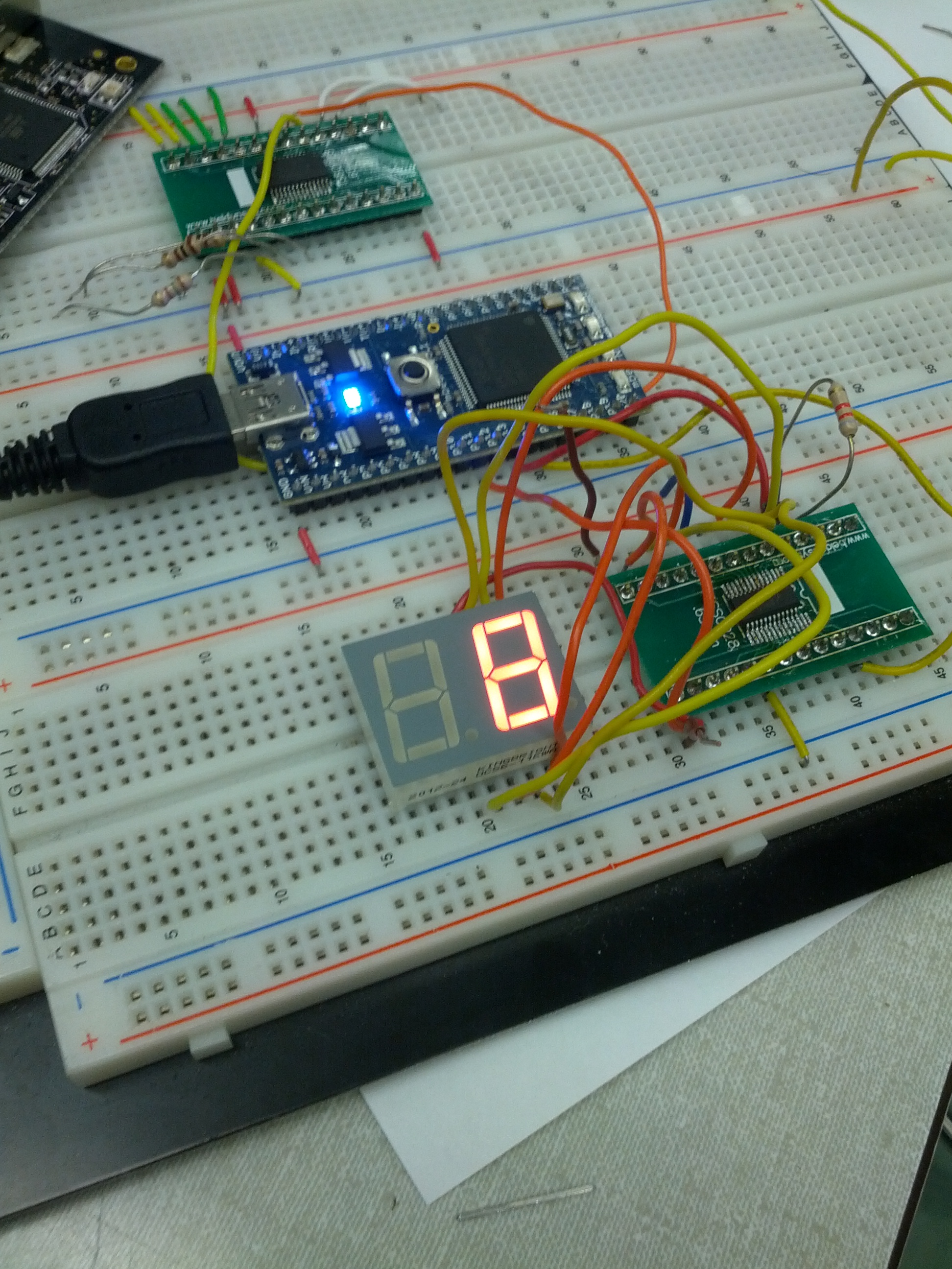
February 21, 2013 (12 hours): Began soldering some parts to test. Soldered and checked connections on the AS1116 LED
driver. The chip seemed to be connected properly to the breakout board. Worked with Josh to get the chip to respond using the MBED. We were able
to have the chip successfully respond to SPI read commands. This was verified using the TLA. The chip was unable to drive any 7 segments at this
time. Attempted to test an i2c slave setup on the Atmel. Atmel does not support a clean way to use slave mode in I2C. Will need to get info from
Spencer to see how to test the Atmel using the Pi as an I2C master.
February 22, 2013 (4 hours): Successfully interfaced the AS1116 with the MBED (Finally). This was done by rechecking
the wiring and uneccesarily initializing several registers on the AS1116. Tested the driver in full scan mode. This means that the driver will
cycle through eight 7 segments and coincidentally, each segment will only be on 1/8 of the time. Unfortunately, the segment was very dim under
these conditions. Overlaying a piece of the thicker 0.118 inch Acyrlic over the seven segment display rendered it a little fuzzy and difficult
to read. Wrote up some code on the Atmel to test the AS1116 using our micro. Looked at several choices for oscillators in order to clock our
micro faster.
February 23, 2013 (10 hours): Continued work on using SPI on the Atmel to control the AS1116 driver.
Disabled the pins from ioport mode and set them to SPI mode. Tried using the SPI driver in Atmel Studio, rather than the service. Set SPI
to set a chip select signal (being used as LOAD on the AS1116) low each time it begins sending data. The CS0 signal remains low until it has
sent out data to all five drivers. Then the chip will be deselected and CS0 (LOAD) will be driven back to high. Using the TLA, it was pretty
obvious that the pins were not outputting anything yet. Will have to return to this issue tomorrow. Attempted to set up the micro to
use an external oscillator, and set the PLL to divide the clock. Using a 5MHz square wave as input to the XIN0 pin, the PLLOSC was set to
OSC0. PLLMUL was set to 11, and PLLDIV was set to 0. By the equation f = 2*(PLLMUL+1)*fin if PLLDIV=0, we should be getting 24 times the
input frequency, or 120MHz on the PLL which fits well within the 80 to 240Mhz range of the PLL. The system clock was then set to use the
PLL output. This process will have to be fully debugged tomorrow since its getting pretty late.
February 24, 2013 (4 hours): Made a lot of effort in setting up the PLL to divide the osc0 input clock.
So far no success on getting the PLL to work for our micro's system clock. Wrote a RGB driver test to cycle through the RGB colors using the micro
and recycling code used to program the mbed earlier. Luckily we finally have our micro controller interfacing with something!
Started work on soldering a prototype hexagon so we can test the hall effect sensors with the proper distance they will have between them.
WEEK 07 SUMMARY Accomplishments: Progress on using the PLL and AS1116 driver, and test code on the micro for the RGB driver Weekly Work Total: 31 Project Work Total: 97
Week 08
March 2, 2013 (6 hours): Josh and I were successful in using the PLL and an external oscillator to set the
system clock in the micro controller. Wrote a simple "Heartbeat" program that will test the micro when we first begin to populate the
PCB.
The simple RGB driver was modified so that it would cycle through colors for all the LEDs on the board. Now we have test code that
is verified to work so we don't have to debug our drivers and the PCB at the same time. This was accomplished by writing instructions
to address 7, which will send the commands to all the RGB drivers.
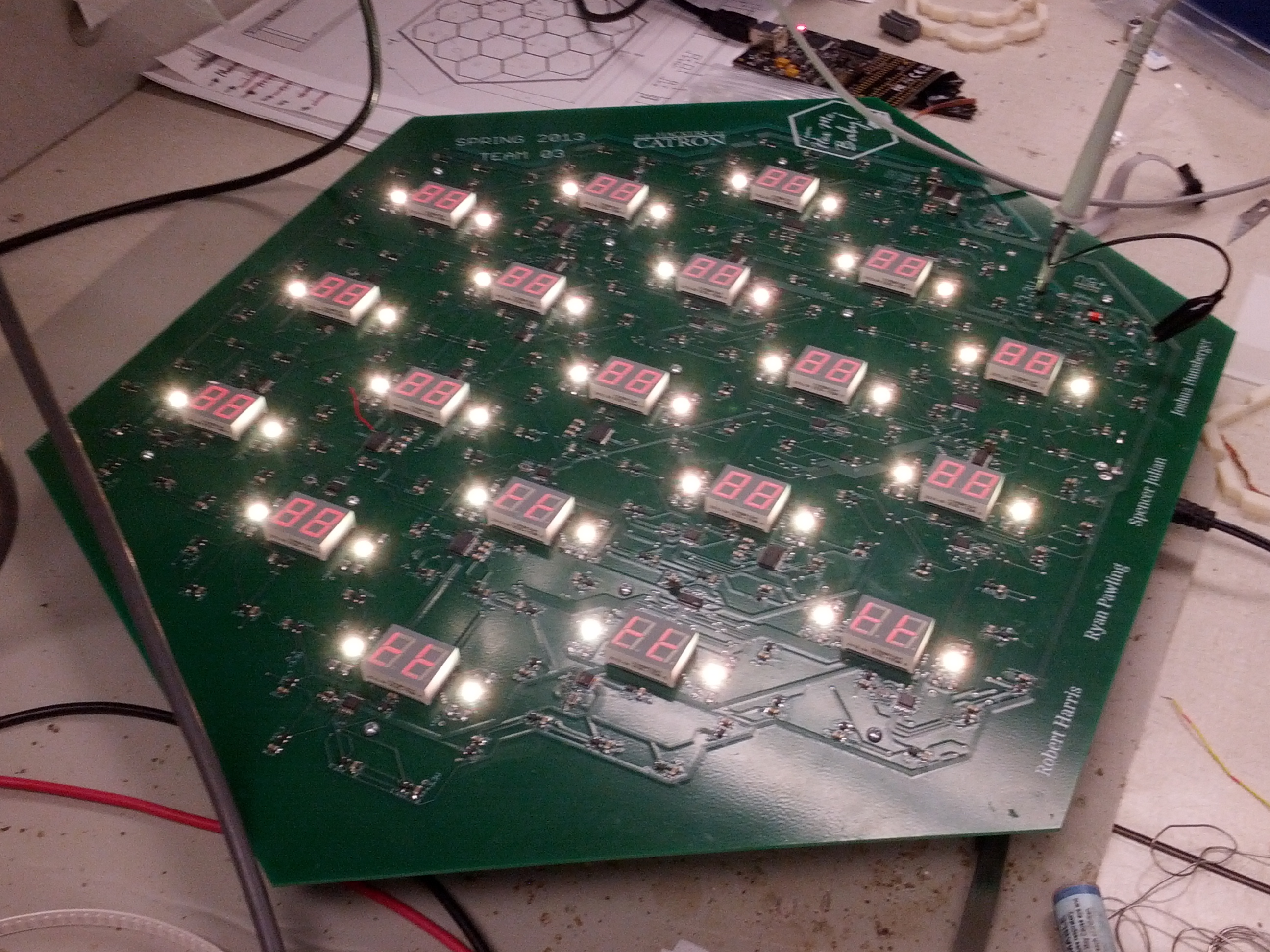
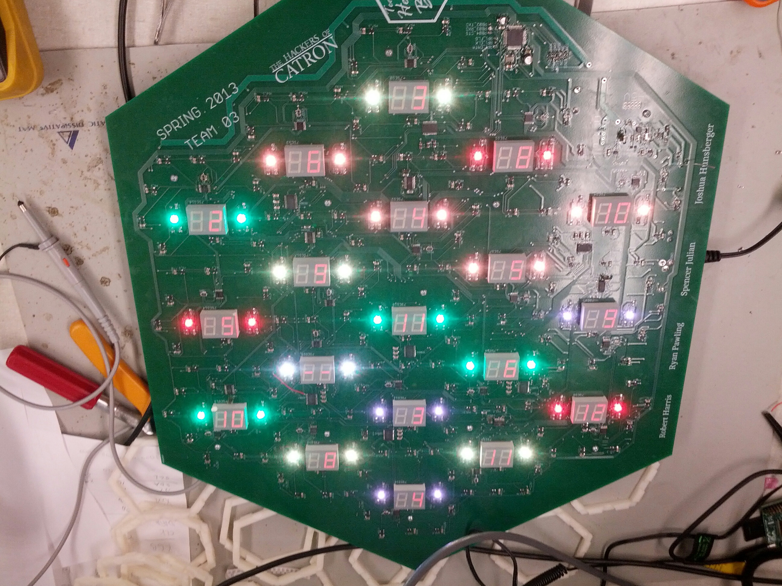
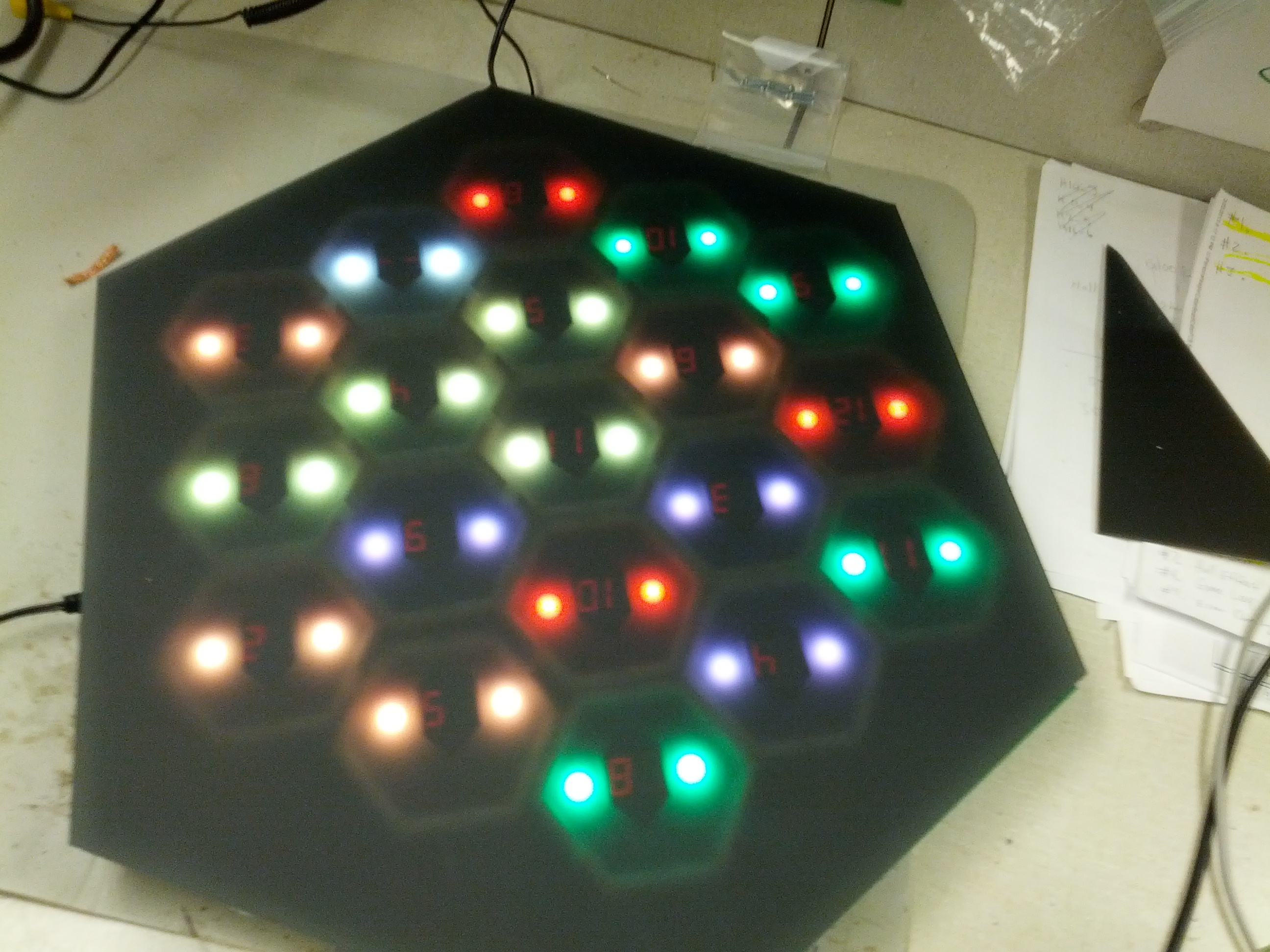
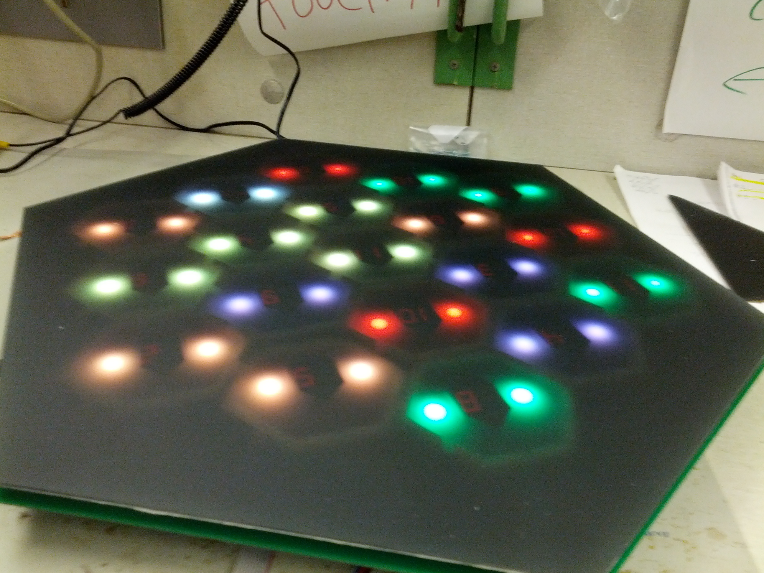
Created test code for the 7 seg driver on the Atmel. The code initializes all the drivers to the settings we want and displays an 8
on each one so we can easily check for correct soldering on the PCB. This was done using SPI communication with the driver. SPI
is set by initializing gpio to map the pins and function we want to use. The baudrate was initialized to 2Mhz and the chip select id was
of the 7 segment drivers was set to 0. This means that each time micro writes instructions to the drivers, it sets the chip select
(LOAD) line low. The micro will send at a string of five instructions, one for each driver. Then the chip is deselcted, driving the load
line high and latching the data in the drivers. This means each time we want to address a seven segment, we must write out five instructions
so that it can shift all the way through the string of daisy-chained drivers. The driver was activated by setting it to normal operation, setting
the intensity high, the scan limit to 8, and digits 0-7 to 8.
Finally, we decided to combine these tests by making a test that synchronizes the RGB light cycle with the 7 segments which count 0-5
March 3, 2013 (3 hours): Continued work on getting I2C to communicate between the Raspberry Pi and the micro. This
is done by setting the Pi in master mode and setting the micro in slave mode. Unfotunately there is no nice 'service' to use for the micro in
slave mode, so we had to find and modify an example code using the Atmel as a TWI slave. We were successfully able to interface the Pi and the
micro by constructing a USB power supply for the Pi that shares common power and ground with our board. Used the command 'sudo i2cdetect -y
1' to check the i2c databus for any slave devices. It showed that there was a device at address 50 which is exactly what we set our micro to.
WEEK 08 SUMMARY Accomplishments: Used the PLL and external oscillator to set the frequency of our device to 60MHz.
Inferfaced with the 7Seg driver and RGB driver by writing test code that we can use while we populate our PCB.
Successfully interfaced the Raspberry Pi with the micro using I2C. Weekly Work Total: 9 Project Work Total: 105
Week 09
March 5, 2013 (2 hours): Completed work soldering and testing connections on the example hex. Will be sure to write up
some test code in order to test the distance between hall effects for our chosen magnets, sampling hall effects using the micro, and how the lights
disperse at their given distance. This will be done later this week if there is time.
March 6, 2013 (2 hours): Discussed with the team what will need to be thinking about as we build up our software after spring
break, what states the micro should have, and when the micro and pi will communicate.
WEEK 09 SUMMARY Accomplishments: Sample hexagon completed, plans for the software have begun. Weekly Work Total: 4 Project Work Total: 109
Week 10
WEEK 10 SUMMARY Accomplishments: Spring Break. Absolutely nothing Weekly Work Total: 0 Project Work Total: 109
Week 11
March 18, 2013 (1 hour): Met as a team to discuss how the board will notify players of incorrectly placed pieces.
Developed a solution which involved lighting up the hexagon that contains the misplaced piece and displaying on the Pi an image of the piece to
remove/replace. However, we realized there is a more efficient way to solve this without using the Pi. The board will light up the hexagon that
the piece is located on. The seven segment will display a letter to identify the type of piece that needs to be replaced and a combination of
segments to determine the position. Josh's lab notebook contains a picture example of what we intend to display
HERE.
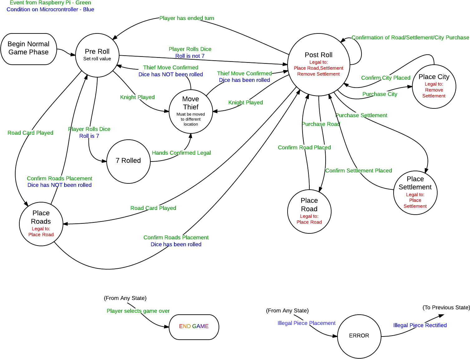
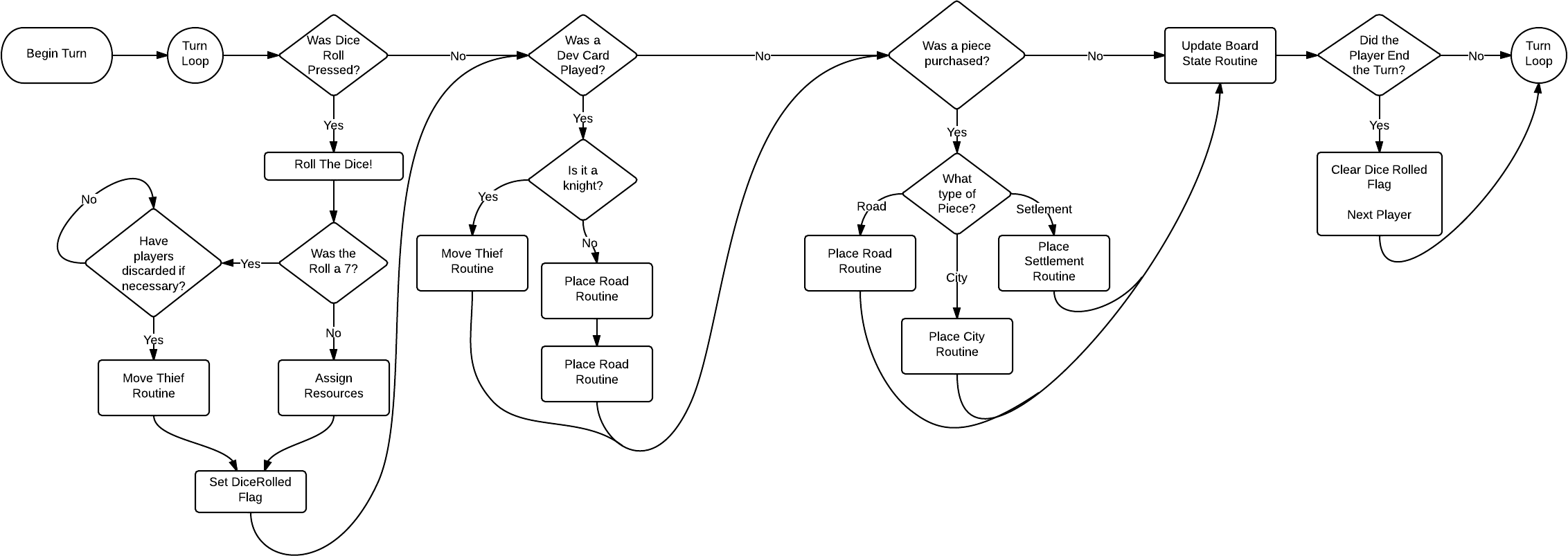
March 19, 2013 (5 hours): Met to work out the flow charts we will be using for the software design. Mainly
focused on the main game loop. Will need to flesh out some of the subroutines later. The original design is an event driven state machine
where the Pi will trigger an interrupt (green text) and the micro will check a condition (blue text). The red text represents what piece
placements are legal during these states. If an illegal piece is placed, there is a software triggered interrupt that traps in an error state.
This approach had many flaws but it let think of what sorts of problems we would have with players moving and removing pieces at anytime during
play and how to detect and prevent that. We developed a much simpler (and more effective) polling game loop (which will sit in main).
The micro will poll the i2c registers to check for various events. When the events occur, the main loops calls the needed subroutines to handle
the event. When main reaches the end of the loop, it will check the board state which essentially looks for misplaced pieces and forces players to
remove them. If there are no misplaced pieces it looks for new legal pieces and asks if the player would like to buy them. Please see the images
below for clarification. The image to the right is the man loop design we plan to use. The image to the left explains what types of pieces can
be placed at what times.
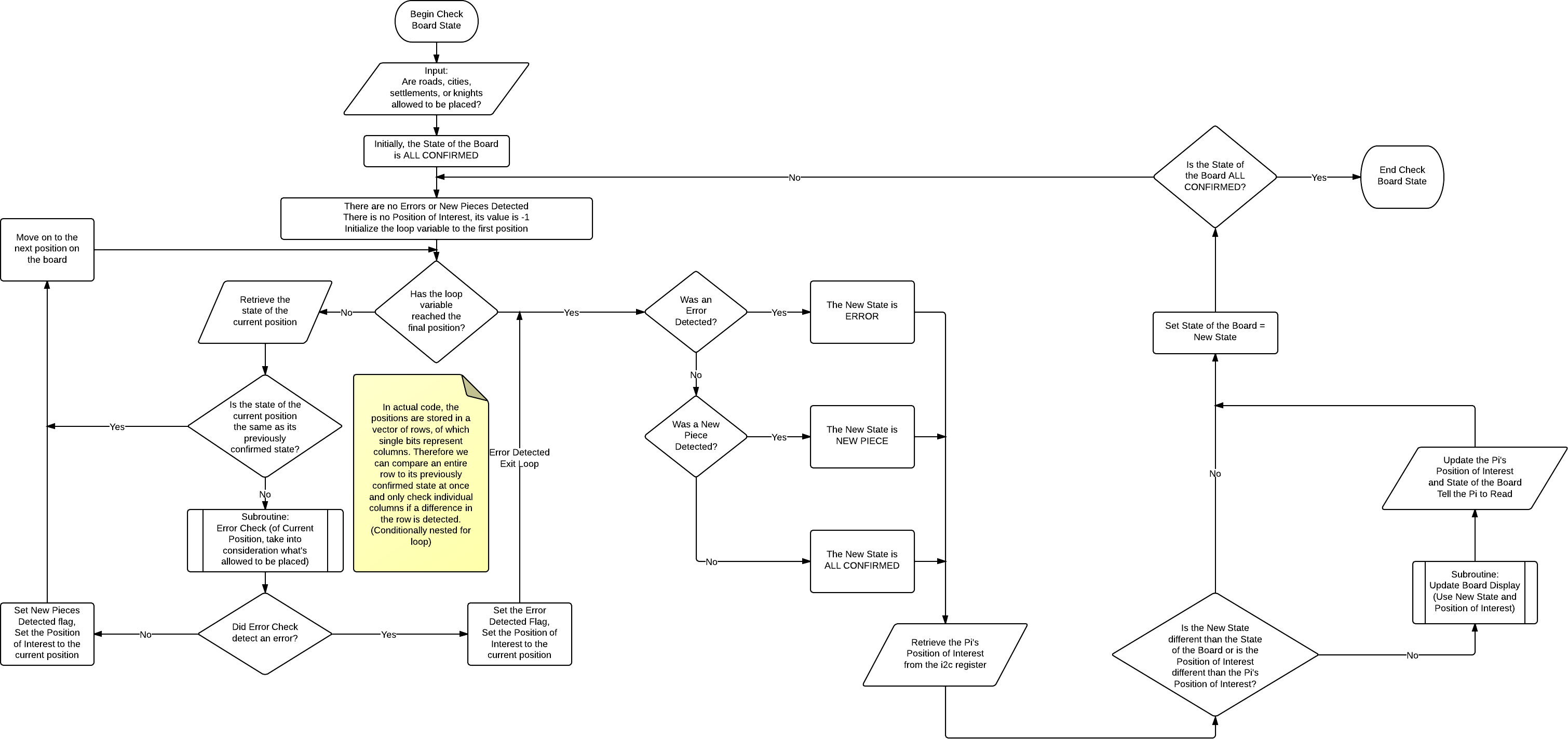
March 20, 2013 (4 hours): Worked with Josh to test the power on the PCB and design a flowchart for the Check
Board Status Subroutine, which first will fix errors in piece placements on the board, then send potential legal piece placements to the
Pi to be purchased and confirmed. This is accomplished by polling all the hall effects and checking whether their new state is different
than their previous state. If so, the position is checked using a set of game-specific parameters to decide whether it is a legal or illegal
placement. If it is illegal, it enters a trap state until the player fixes the problem. If it is legal, the position of the piece is sent to
the Pi. Please see the picture below for the full flowchart.
March 22, 2013 (3 hours): Worked more with the i2c protocol to figure out how to write to memory in the microcontroller. We will
use this memory as registers that the micro will check to see what events have occured on the Pi. The micro can also write to the registers and trigger an
interrupt line which makes the Pi read whatever the micro is sending. The master device Pi sends a 3 byte address to the micro. Once this has been received,
all following bytes are considered to be data and will be written contingously in the memory. This is useful if we want to write to multiple registers in the
micro at once. We still haven't decided how we are going to organize these registers or the exact data we will be sending between the Pi and microcontroller.
March 23, 2013 (4.5 hours) : Work on a rand function in order to calculate the dice roll and produce random setup of the game
board. Tried to use the DSP module to create an undeterministic random number but the module would not load into atmel studio. Tried to use rand() but it
would generate the same random numbers every time on startup. Also tried writing to flash so that we could increment a seed each time so that the
board will be different. Settled on using the cycle timer on the micro to seed the rand() function. At the team meeting discussed the soldering timeline,
software development timeline, and materials and parts needed. Some acrylic samples were ordered to see if we could find a better material to disperse the
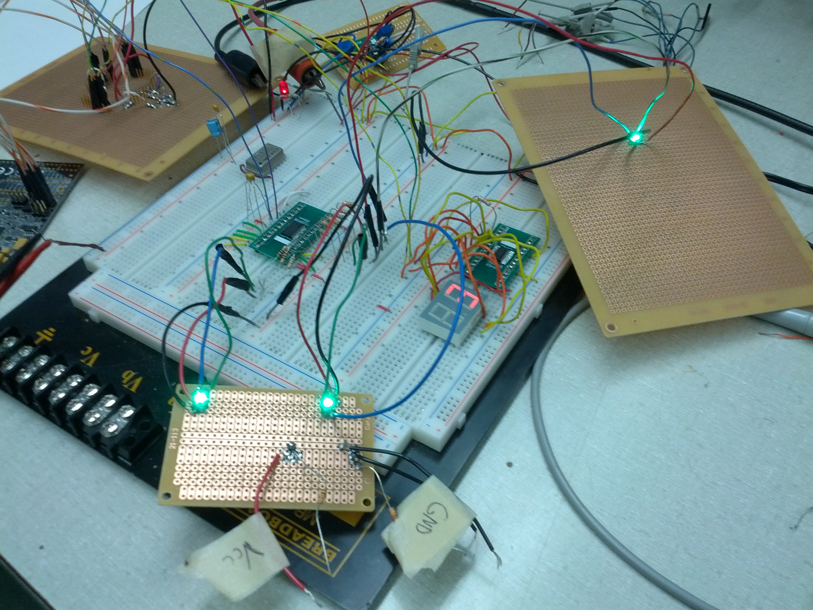
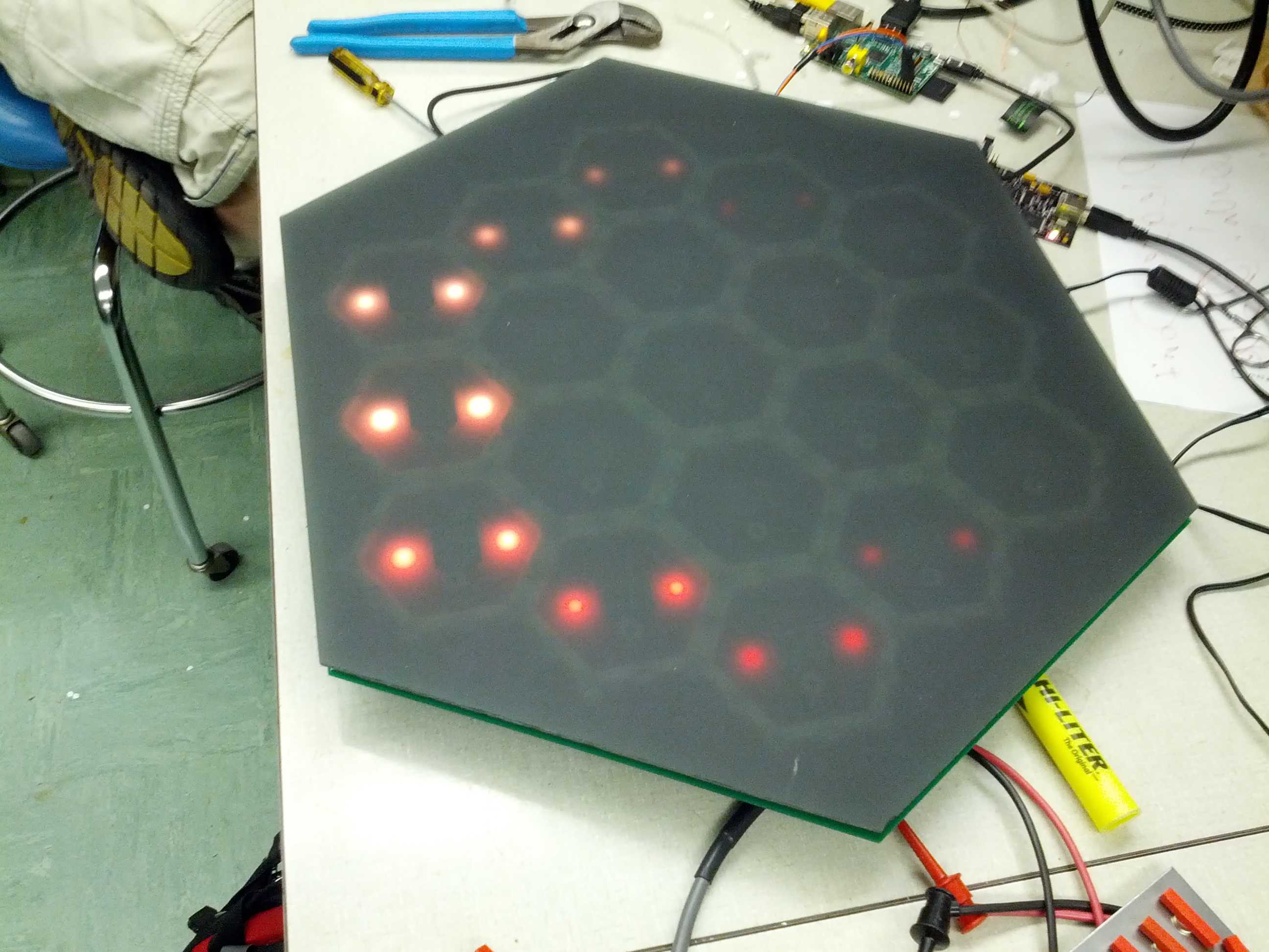
LED light. Soldered the Hall Effect sensors in for one mux and tested them successfully.
March 24, 2013 (5 hours) : Worked with Josh on the static map we will be using to store each position and its type, adjacent positions,
and adjacent hexes. This must be done since there is no easy way to organize the board as a grid, so the mapping must be relational. After this continued soldering
the hall effect sensor network by finishing 4 hexes. There are only 7 left!
WEEK 11 SUMMARY Accomplishments: Received PCB, soldered in the power and micro circuits, tested several RGB LEDs and drivers. Progress on i2c getting
the micro and pi to send messages to each other. Developed several flowcharts are we plan our software design. Team meeting to plan
out our timeline to completion. Packaging material samples ordered. PCB almost 50% complete. Weekly Work Total: 22.5 Project Work Total: 131.5
Week 12
March 26, 2013 (4.5 hours) : Continued work on PCB to finish soldering all the Hall Effect sensors. Modified to test code to verify all
sensors in sequence, including the extra hall effect #144 which is not in the array of muxes. As I was testing them, many hall effects seemed to be not trigger correctly
or have multiple triggering at once. The measure voltage on the output pin was between power and ground (~2.2V). I checked the resistance across the power and output
of each hall effect find many had on the order of 1 MOhm of resistance. Several of the hall effects were disconnected from the pull up resistor array and the solder
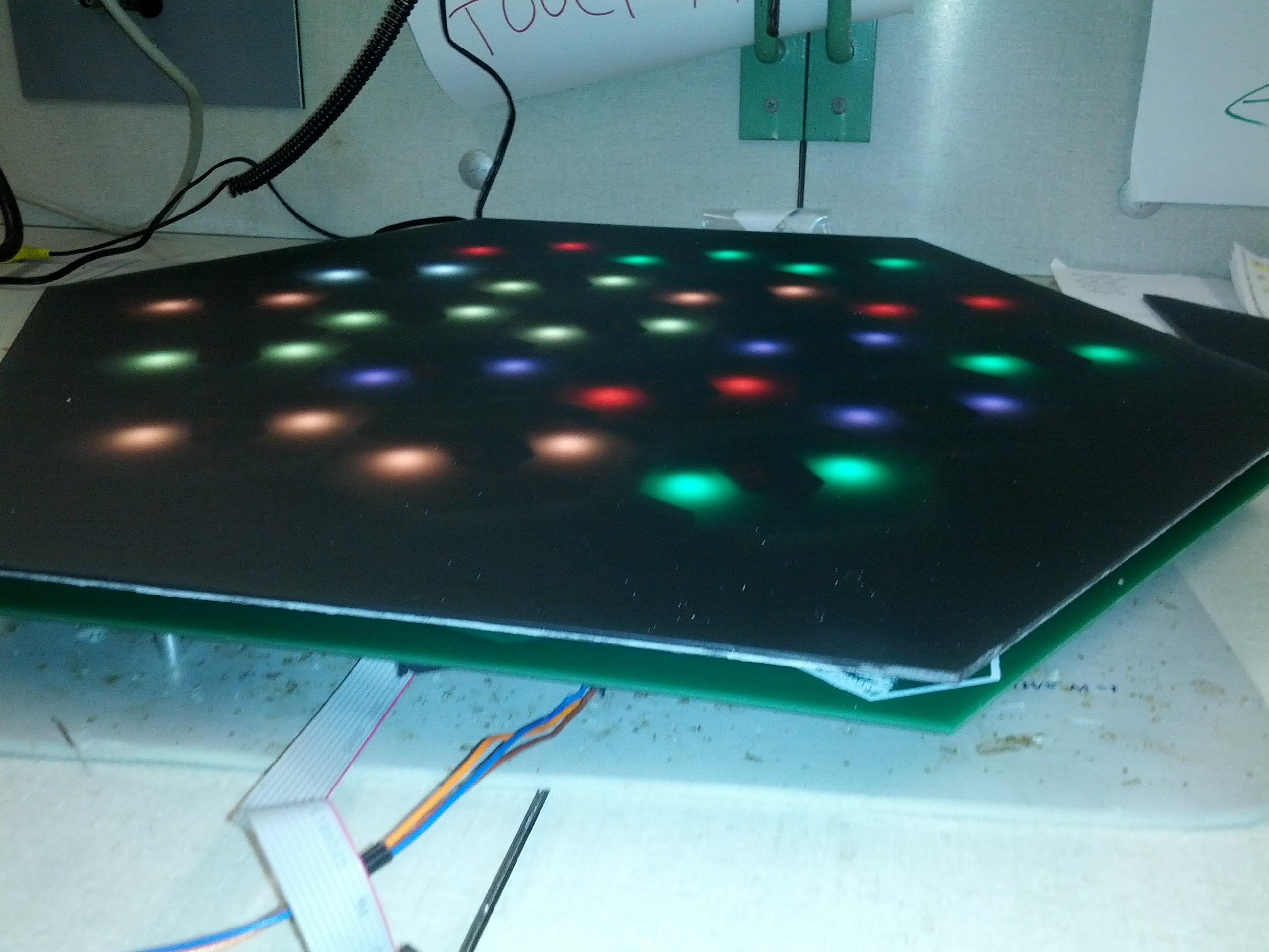
connections had to be touched up. At this point, the hall effect sensor network is fully functional. (picture of finished HE network)
March 27, 2013 (4 hours) : Soldered on one driver for the seven segment display to test. Found that the driver was not working correctly
since the MISO and MOSI lines on the micro had been accidently swapped. Rob and I were able to find a good place on the pcb to cut the traces and put in flywires
to swap the signals. Following that, I began writing some code to abstract the process of writing to the 7 segments.
March 28, 2013 (2 hours) : Tested new acrylic samples, settled on a cool dark grey color we had not considered before. The exterior
of the board will also be made from this. Began to organize all the code initializations into a new project, Catan. Experimented with using different files
for controlling different peripherals.
March 29, 2013 (1 hour) : Soldered on a couple hexes of RGBs, 7 Seg issue arose where the display is erratic and the power supply becomes
unstable.
March 30, 2013 (7 hours) : Began work on organizing code for main board. Wrote a function with hex number and color parameters which maps
the hex number desired with the proper device address and channel address to send via SPI. Found an issue where driver #6 was improperly setup in the schematic so that
it shared an address with driver #4. To fix this, a trace used on driver 4s address pins was cut and rewired to power. This way, driver #4 become driver #6 to fix the
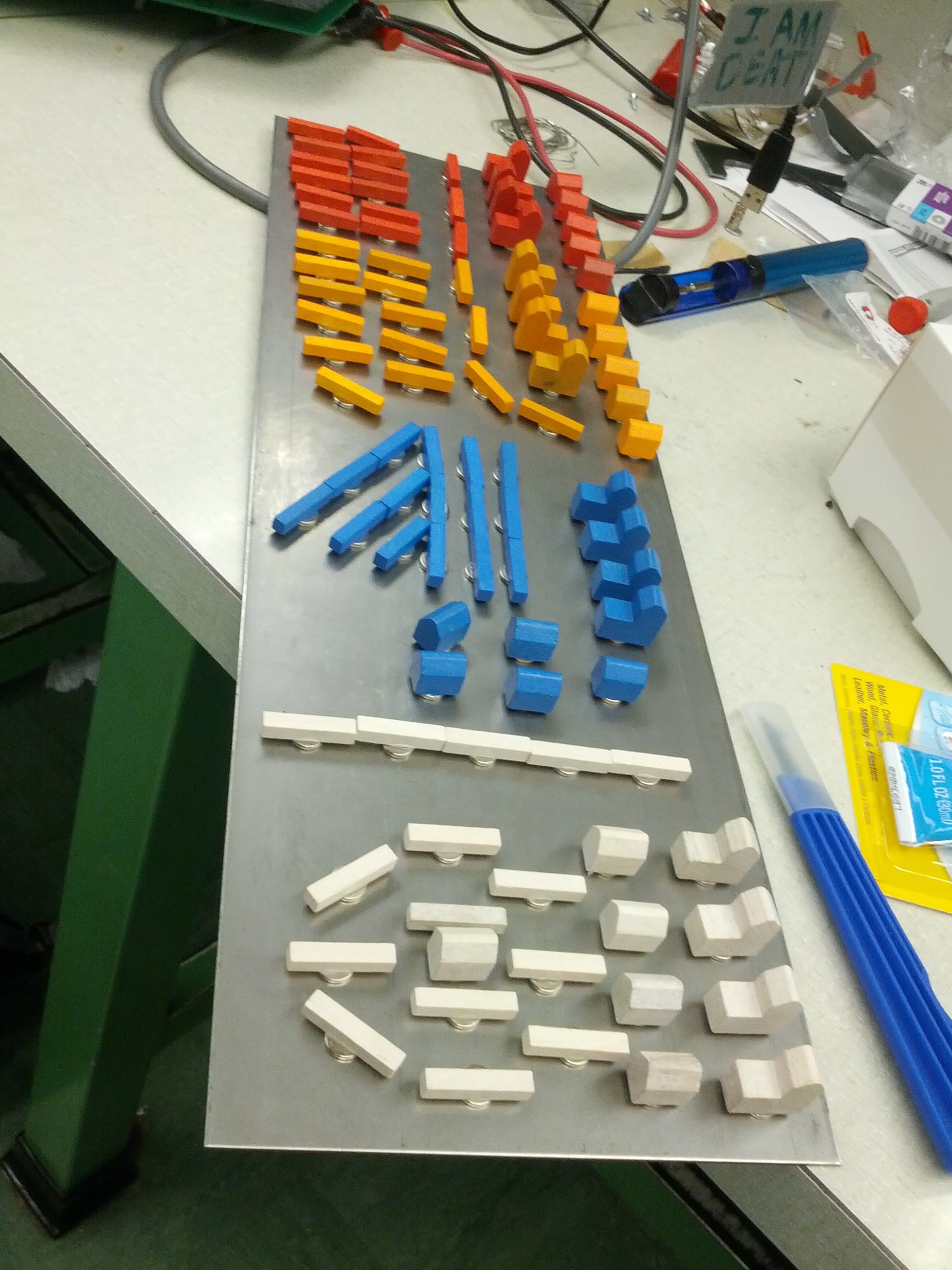
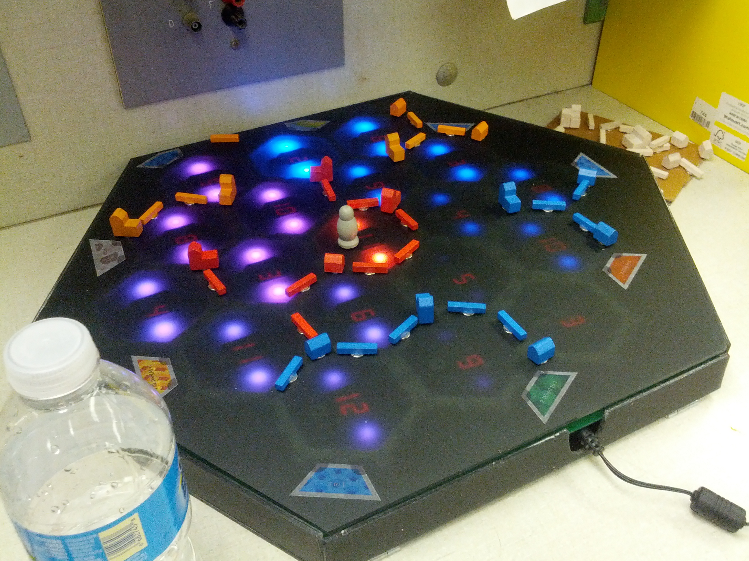
addressing problem. Experiemented with the RGB color choices to find the best color/resource pairs that the team could agree on.
The 7 segment displays still continue to be problematic unless the display brightness is greatly reduced. Using the Oscilloscope, it is evident that
the power supply becomes very noisy once the 7 segments are all drawing current. Hopefully with some additional decoupling caps on the 3.3V power line will allow us
to bump up the brightness a little and make them more readable. Its seems that we have worked out any bugs
in our PCB at this point and can move on to getting the main program going.
WEEK 12 SUMMARY Accomplishments: PCB is basically 100% complete, many PCB issues debugged, work on Game code started Weekly Work Total: 18.5 Project Work Total: 150
Week 13
April 2, 2013 (8 hours) : Worked on the Reliability and Safety Analysis report and presentation. Very exciting.
April 3, 2013 (4 hours) : Worked on the Reliability and Safety Analysis report. Worked with Spencer on the board generation algorithm to
randomly select a starting tile to place rarities across the board. It this point, board generation is complete, but we are looking for a different way to give the
board a random number, rather than swiping a magnent across it and getting the timer count. There is a strange error in the resource generation that sometimes causes
a glitch where the remaining tiles become ore. We may or may not have fixed it, it is hard to tell since the glitch rarely appears.
April 4, 2013 (3 hours) : Finished the reliability report.
April 5, 2013 (5 hours) : Integrated the static maps into the software. The purpose of these maps is to match each position
on the board with its adjacent positions, adjacent hexes, and ports. Even numbered positions represent the roads, odd numbers with the exceptions of
those evenly divisble by seven are settlement locations. The positions that are divisble by seven represent the locations the theif can be placed. The data
structure is a 2D static array which takes a position as the first index and a data field as the second index. The first three data fields correspond to
adjacent positions, and the second three correspond to adjacent hexes. The seventh data field is reserved for ports. A separate array was created to store the owner
of each position on the board since this will not be static. A test was created which lights up adjacent hexes of each position when a piece is placed over it. It also
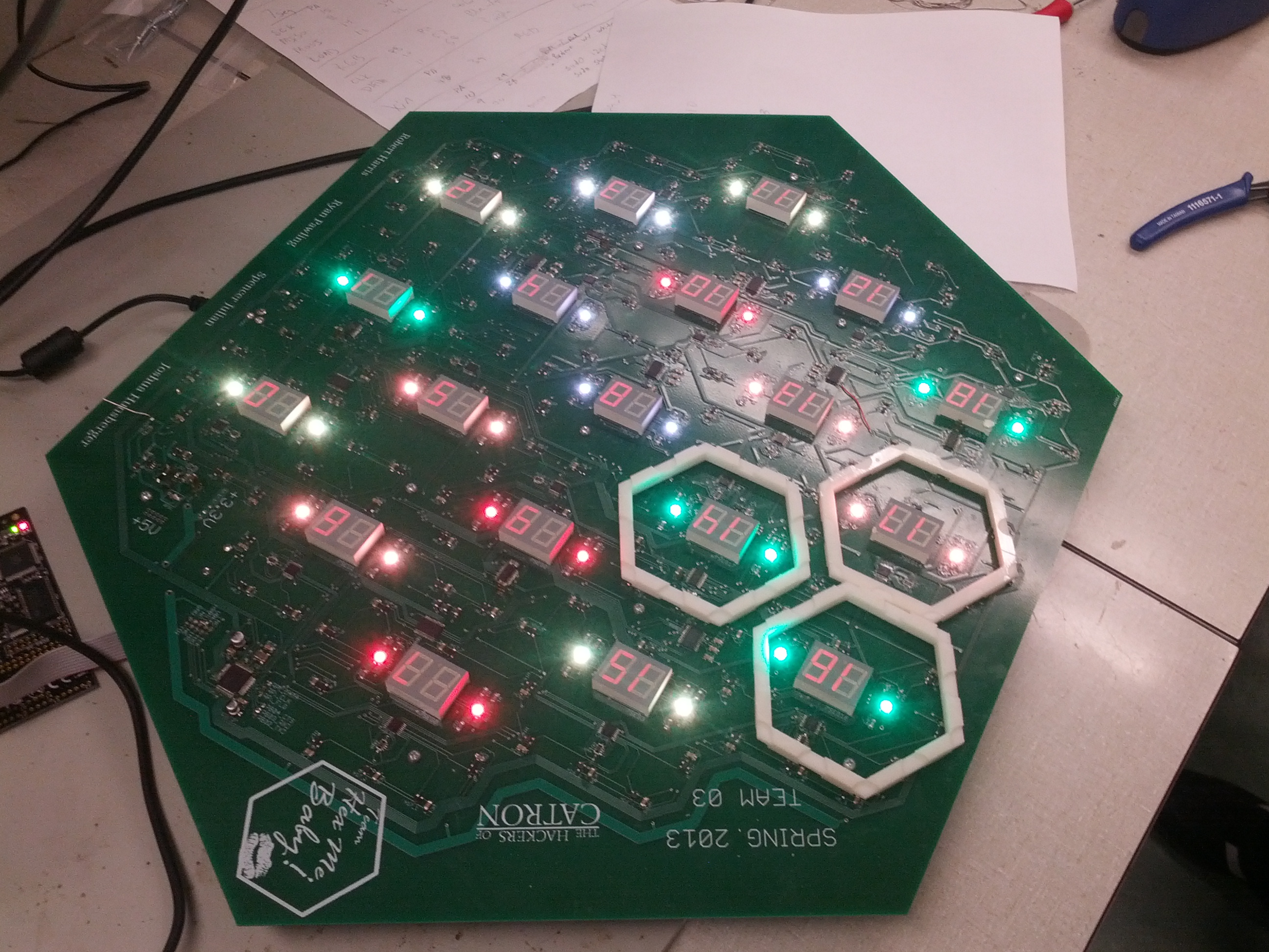
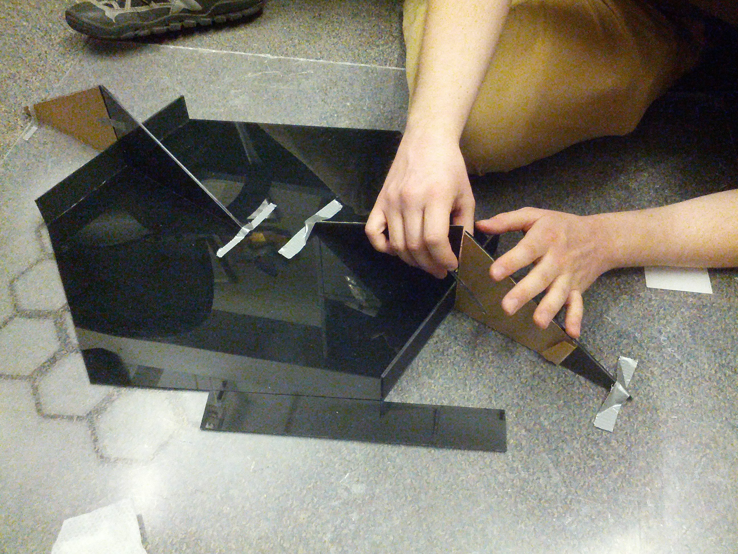
uses error codes to point to each adjacent position. This test helped to verify that the mapping was correct. Packaging construction has begun.
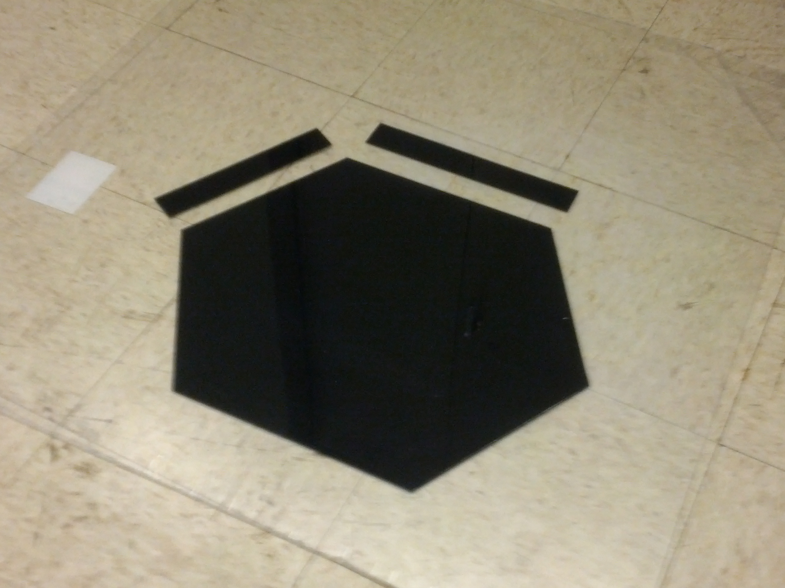
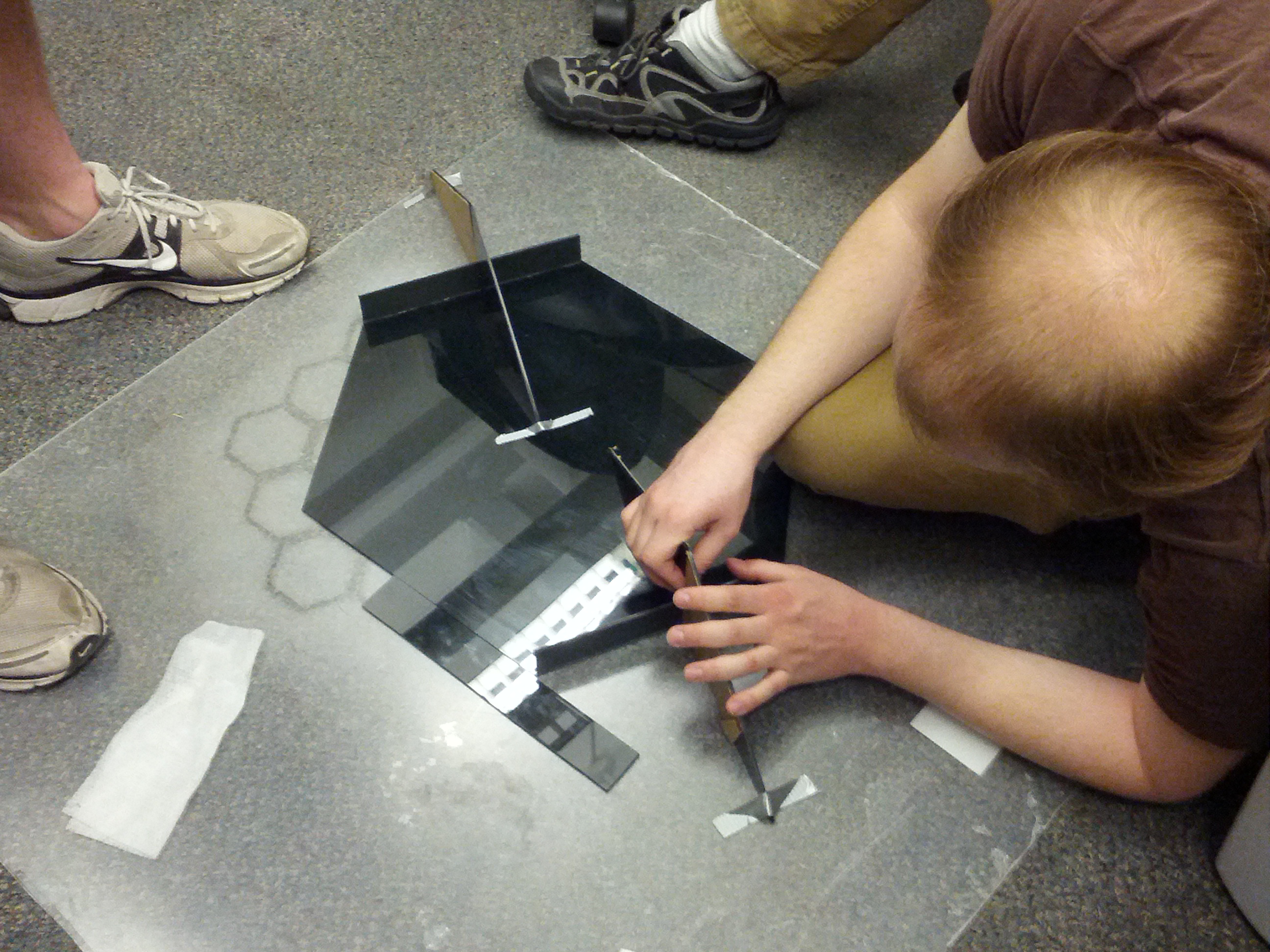
Three sheets of black satin ice acrylic arrived. Josh, Spencer, and I scored and cut these pieces to make the top hexagon shape and bottom hexagon shape.
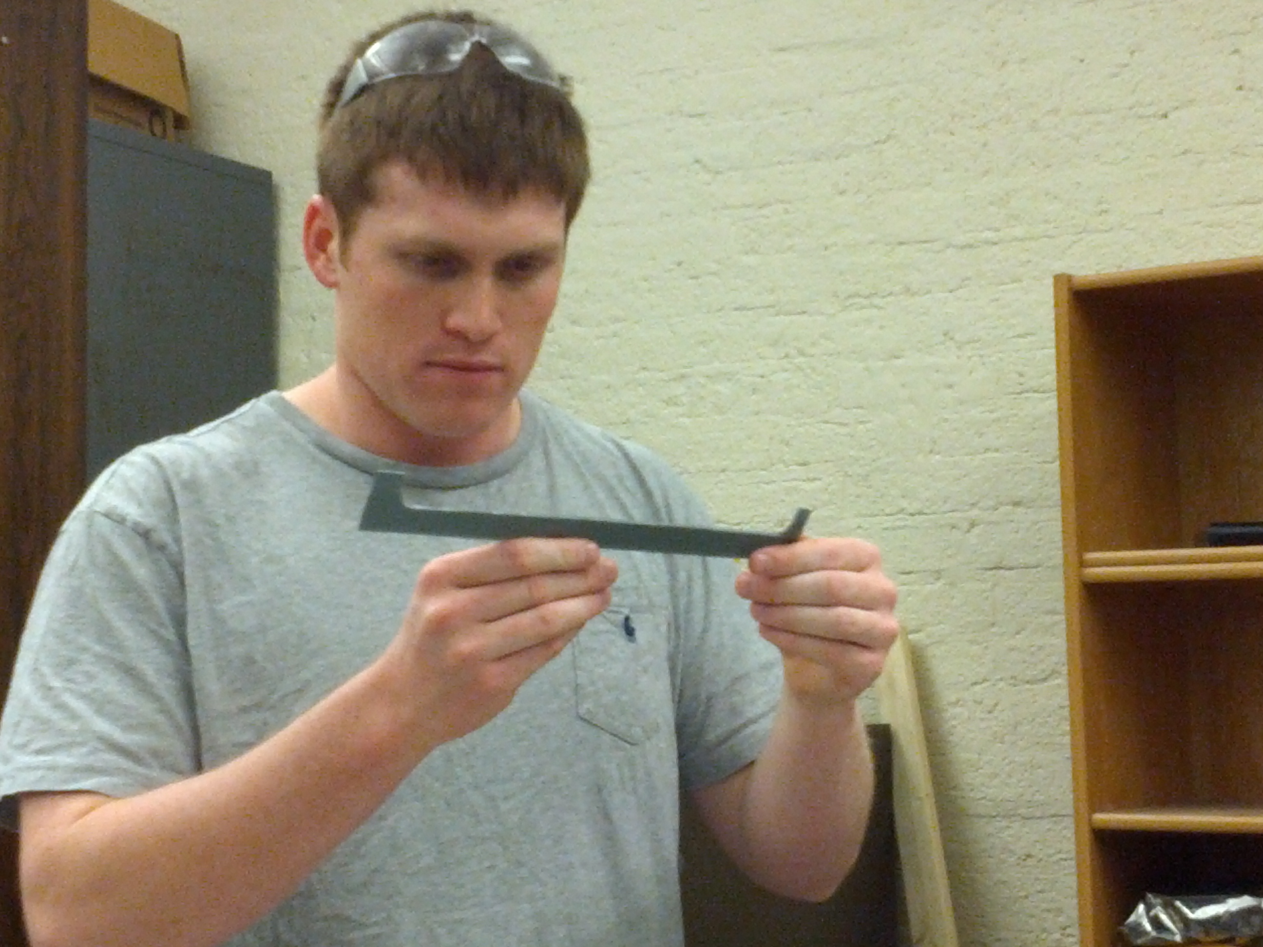
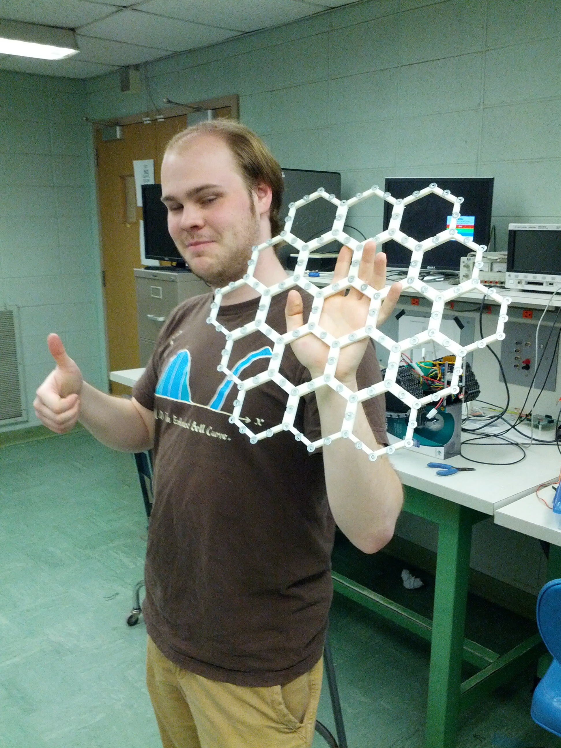
April 7, 2013 (6 hours) : Work on packaging has continued. With the help of Spencer and Rob, each of the ABS plastic hex dividers was glued
together with washers in the recesses in order to attract the magnetic pieces. Work began on the packaging exterior as sides where carefully glued to the base and
supported while they dried. A dremel was used to sand down the rough edges on the cut acrylic, as well as to sand away an indent into the door for switches and power
cables to be exposed. With much difficultly, the hex divider grid was glued using adhesive spray to the top sheet of acrylic. Packaging construction is nearly complete!
WEEK 13 SUMMARY Accomplishments: Reliability and safety analysis is complete, static mapping of positions finished and tested, packaging nearly complete. Weekly Work Total: 26 Project Work Total: 176
Week 14
April 9, 2013 (5 hours) : Worked with Josh on the main game code. Added functionality for ports and changing and checking the game state. Began work
on what would be needed to confirm a new piece. Completely finished board generation, which is triggered when the rpi writes a start bit (0x01) to the event register (0x00). Prior to
this, the rpi will write random data to registers 0x09 through 0x1c. This data can be used to randomly generate the board if the player has not already manually done it themselves
while playing with the board's interractive wait stage during boot-up.
April 12, 2013 (5 hours) : Wrote IsValid, which checks based on the rules of the game whether a piece is
legally or illegally placed. Check game state checks all the sensors to see which pieces are new. These pieces are checked for
their validity and sent to the rpi to be confirmed. When the rpi confirms a new piece, it is added to the game state.
April 13, 2013 (5 hours) : Check game state routine completed and verified. Wrote functions to build roads,
settlements, cities, and move the thief.
April 14, 2013 (6 hours) : Worked with Spencer on I2C commmunication between the rpi and micro. Created an "on" animation
on start of the micro to notify the player that the board is on and can be played with. After the pi has been booted, a waiting animation plays while
player connect to the webserver. The error/confirm display now displays the color on all adjacent hexes. Added a functions to give players their initial
resources during the 'place initial settlements stage of the game'. Wrote the main game loop which checks the state of the board and various pi registers
for events. See the flowchart from March 19 for more info on the main game loop.
WEEK 14 SUMMARY Accomplishments: Weekly Work Total: 21 Project Work Total: 197
Week 15
April 16, 2013 (9 hours) : Worked with Josh to debug the main game loop and communication with the rpi. Also began work
on the longest road algorithm.
April 17, 2013 (3 hours) : Finished work on the longest road algorithm, also some testing was done using the webserver.
Bugs were worked out all the way through initial setup, but some errors are still occuring during the main game loop.
It was decided that the web is too slow for our purposes with about 10 seconds per action, and Rob and Spencer decided to rebuild it from the ground up.
April 18, 2013 (1 hour) : Worked with Josh on the initial poster design
WEEK 15 SUMMARY Accomplishments: Code on the micro is essentially complete, potential bugs aside. Poster complete. Weekly Work Total: 13 Project Work Total: 210
Week 16
April 23, 2013 (12 hours) : Worked with Josh on post game reset of the micro using a watchdog timer. Experimented with colors
to find the best colors to match the web app and represent the resources. Also, printed and cut the labels
used to mark the ports on the playing surface. Wrote an animation to play at the end of game. Filmed the PSSCs and stayed up very late editing a video displaying them.
April 26, 2013 (5 hours) : Worked with the team to work out some of the kinks with the game
before the design showcase. Displayed the project and presented it to curious 270/362 students.
April 27, 2013 (2 hours) : Worked with Rob on the Senior Design Report.
April 28, 2013 (4 hours): Worked on the final report, play testing the game
April 29, 2013 (6 hours): Finished the final report, updated lab notebook, finished peer reviews
WEEK 16 SUMMARY Accomplishments: Weekly Work Total: X Project Work Total: 210 + X