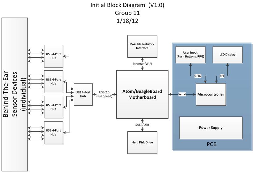
Completed preliminary system block diagram (V1.0)
System Diagram:
January 11, 2012 (1 hour):
Met with professor Talavage to discuss the basic
functionality of the headset sensor devices that will be used to collect data for this project. Discussed
challenges of interfacing these devices to the base station using the USB protocol standard.
January 11, 2012 (1 hour):
Met as a team to complete preliminary project proposal.
January 12, 2012 (3 hours):
Researched USB protocol standards. Determined that the
base station must have some sort of USB host to communicate with the USB sensor devices. Discovered that it would
be much easier to implement USB communcation protocol with a motherboard rather than a bare microcontroller.
WEEK 01 SUMMARY
Accomplishments: Submitted preliminary project proposal. Gained insight into
USB protocol standard, and determined a motherboard would be ideal to handle USB communication.
Weekly Work Total: 5 hours
Project Work Total: 5 hours
January 18, 2012 (1 hour):
Met with Professor Vijay Raghunathan to further discuss
project idea. Professor Raghunathan suggested using a BeagleBoard running embedded Linux as primary means of
USB communication. The BeagleBoard would also be able to interface to a hard disk, maintaining the file system
necessary to hold data obtained from several headset sensor devices.
January 18, 2012 (3 hours):
Met as a team to discuss PSSC's for this project as well as
system design. The current plan is to cascade powered USB hubs to support up to 16 USB headset sensors, which will
connect to a USB port on either a BeagleBoard or Atom board. This board would also manage a file system on a hard
drive disk used to store data from the headsets. A standalone microcontroller would be used control an LCD display,
as well as power some LEDs and interface with the user through pushbuttons and a rotary pulse generator. The standalone
microcontroller would communicate with the motherboard through a serial interface. Also, it was decided that the
group would utilize Trello as a free project management service for this semester.
PSSCs:
1. An ability to obtain raw data from sensors via a USB interface with motherboard
2. An ability to store raw data and manage files on mass storage device
3. An ability to charge and monitor sensor battery status and convey to the user
4. An ability to receive user input and interface to the user through graphical display
5. An ability to communicate to the motherboard via the microprocessor using serial interface
January 18, 2012 (1 hour):
Completed preliminary system block diagram (V1.0)
System Diagram:
January 20, 2012 (1 hour):
Met with Professor Johnson to discuss concerns related to the proposed design
meeting 477 course requirements. Johnson expressed that he thought the project placed too much functionality on the motherboard,
leaving little functionality for the custom PCB. It was concluded that either a much larger portion of responsibility would need
to moved from the motherboard to PCB, or a new project idea would need to be developed.
January 20, 2012 (2 hours):
Met with George Hadley to discuss the possibility of moving USB host
functionality from the motherboard to the PCB. George felt that amount of work required to achieve this would be much too great
to fully complete the design by the end of the semester. The team concluded that a new project idea would be a much better idea than
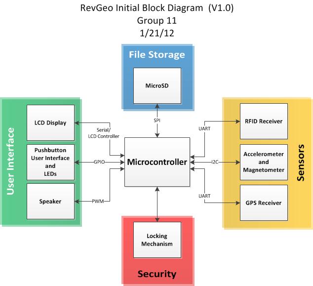
trying to modify the original idea. It was concluded that the new design would be a "Reverse Geocache" device, where instead of
locating a box using gps coordinates, there would be a box that would remain locked until it had been brought to the correct sequence
of GPS locations.
January 21, 2012 (4 hours):
Met as a team to discuss theory of operation for the new project idea. It was
determine that the newly named "RevGeo" Reverse Geocache would receive GPS signals to determine its current location, direct its user
to the next "checkpoint" by the use of LEDs and a compass with tilt compensation, and unlock itself with either a solenoid or servo
controlled locking mechanism when the box has reached its final destination. The box will also have an LCD screen to interface with
the user, read instructions from a microSD card, and a speaker to play audio when the box unlocks. Finally an RFID "master key" system
will be implemented to override the system and unlock the box at any time. A new preliminary system diagram was also developed during
this meeting.
New System Diagram:
New PSSCs:
1. An ability to obtain and decode global positioning data via GPS
2. An ability to decode acceleration and magnetometer data to determine a compass heading
3. An ability to access and interpret files located on a microSD card
4. An ability to display information to the user via an LCD display
5. An ability to identify an RFID tag using an RFID reader and serial interface
WEEK 02 SUMMARY
Accomplishments: Project proposal, block diagram, and PSSCs created for initial idea, then revised to reflect
new project idea.
Weekly Work Total: 12 hours
Project Work Total: 17 hours
January 23, 2012 (3 hours):
Worked through Sparkfun Eagle tutorials for Schematic, Layout,
and Custom Component Generation. Based off the knowledge gained in these tutorials, the group created a custom component
for the National Semiconductor LM2675M-5 switch mode voltage regulator chip. Using this custom component, a layout and
schematic was individually begun for the 5V regulator circuit described in the PADS tutorial.
January 23, 2012 (2 hours):
The group discussed a preliminary list of major components needed for
the project. Items on this list are as follows: Microcontroller, GPS receiver, compass, RFID receiver, MicroSD card, locking
mechanism, rechargable battery, LCD screen, speaker, case. Began more in-depth research on some of these parts, with the goal
of purchasing many of these parts in the next few days.
January 24, 2012 (1 hour):
Completed the schematic and layout for the 5V regulator circuit
described in the PADS tutorial, and was checked off by the George Hadley for completion of HW #2.
January 24, 2012 (1 hour):
Met as a group to finalize the TCSP presentation slides for tomorrow,
and determined who would discuss each topic during the presentation.
January 25, 2012 (2 hours):
Met as a group to develop a preliminary cost sheet based on the components
be used for the project. The total estimated cost for the design will be around $300. Several parts were ordered during this meeting,
which will arrive by Monday of next week at the latest. Those components are as follows:
* GPS Receiver - Copernicus II DIP Module
(Sparkfun)
* Tilt Compensated Compass (with breakout board) - LSM303DLH
(Sparkfun)
* RFID Starter Kit (RFID module, USB reader, RFID cards) - ID-12
(Sparkfun)
* Speaker - 8ohm, 0.5W
(Sparkfun)
* Pelican Case 1150 - 8.18" x 5.68" x 3.62"
(Amazon)
WEEK 03 SUMMARY
Accomplishments: Completed Sparkfun Eagle Tutorials as well as HW#2, preliminary parts list completed and
several components purchased.
Weekly Work Total: 9 hours
Project Work Total: 26 hours
January 30, 2012 (2 hours):
Researched microcontroller choices for this project. The PIC microcontrollers
from Microchip look to be a good choice, as Microchip has a Memory Disk Drive File System library that allows for easy interfacing with
SD cards. Some other requirements for a suitable microcontroller include having 4+ UART channels, 2+ I2C channels, 2+ SPI channels,
and enough code and data memory for the Memory Disk Drive File System library along with all application code. Taking all of this into
consideration, the PIC24FJ128GA306 looks to be a strong
contender in the choice of micro for this project.
January 31, 2012 (4 hours):
Created and finalized TCSP Powerpoint on Design Contraint Analysis to be presented
in class tomorrow. The microcontroller decided on for this project is the PIC24FJ256GA106,
which has 256KB Flash and 16KB RAM, which will allow plenty of space for application code, as well as for the Memory Disk Drive File System Library
from Microchip to assist with MicroSD interfacing. Also, the PIC24FJ256GA106 has 4 UART, 3 SPI, and 3 I2C, which satisfies the project design contraints
of requiring 3 UART (GPS, RFID, PC Debug), 1 SPI (MicroSD), and 1 I2C (Digital Compass). The team decided to incorportate an
FT232RL IC into the project design, allowing for the device to communicate with a PC via a USB
virtual COM port. PSSCs were also revised to reflect comments from TAs and professors. The revised PSSCs are as follows:
1. An ability to obtain and decode global positioning data in order to verify if current location matches pre-determined desired location.
2. An ability to utilize accelerometer and magnetometer data to determine a compass heading with tilt compensation.
3. An ability to access and interpret files located on a microSD card.
4. An ability to display information to the user via an LCD display.
5. An ability to identify an RFID tag using an RFID reader.
February 1, 2012 (5 hours):
Completed Introduction and Design Requirement sections of the Design Constraint Analysis Homework. For
more details see the "Homeworks" section of the website.
February 2, 2012 (5 hours):
Completed Component Selection Rationale and Conclusion of Design Constraint Analysis Homework, as
well as the initial parts list and revised block diagram. Finalized entire Design Contraint homework. Called up Microchip to obtain samples of the PIC24FJ256GA106 microcontroller. The samples should
arrive late next week.
System Diagram (V1.1):

WEEK 04 SUMMARY
Accomplishments: Completed Design Contraint homework assignment. Finalized and ordered the microcontroller chosen for this
project (PIC24FJ256GA106).
Weekly Work Total: 16 hours
Project Work Total: 42 hours
February 8, 2012 (2 hours):
Met with Chuck to discuss debugging/testing methods for the PIC24FJ256GA106. Chuck supplied the group with an Explorer 16
development board for PIC24 microcontrollers, complete with a PIC24FJ128GA010 for development purposes. Installed the Microchip MPLAB IDE for use with PIC24 software development
and testing, and downloaded the Microchip Memory Disk Drive File System Library for use with interfacing PIC micros to SD cards. Completed a demo tutorial on how to create a new
MPLAB project, connect to the development board, download code, and debug the project on the microcontroller.
February 10, 2012 (3 hours):
Continued to experiment with the Microchip MPLAB IDE that will be used as the development environment for
the PIC24 microcontroller. Began to look at the datasheet for the PIC24FJ256GA106 to identify critical pins for initial programming, debugging, and functionality.
For communication with the ICD 2 Debugger, connections must be made from the debugger to the MCLR (Master Clear) pin, PGEC/PGED pair, and Vcc/Vss. Also, due to the limited
number of pins on the chosen microcontroller, pins for UART and SPI communication need to be assigned funcationality using the Peripheral Pin Select Registers. It seems as
though the user is able to assign input and output pins to a given peripheral without much constraint, which will provide a large amount of freedom when designing the system.
The PIC24FJ256GA106 micros that were ordered last week came in today, and the team talked with Chuck to place an order for microcontroller breakout boards to be used during
initial experimenting and testing stages.
WEEK 05 SUMMARY
Accomplishments: Obtained the main microcontroller to be used for this project. Installed the IDE to be used with the PIC24 micro, and completed initial
tutorials related to creating and building new projects. Began to look at critical pins on micro for initial programming and testing.
Weekly Work Total: 5 hours
Project Work Total: 47 hours
February 14, 2012 (3 hours):
Researched and confirmed how several of the chosen peripherals for this project will interface
with the PIC24FJ256GA106. Since the RFID unit operates on 5V, it was initally thought that level translators would be needed so that the 5V TTL serial
logic could communicate with the 3.3V micro. After further research, it was discovered that the PIC24 device has several digital input pins that are tolerant
up to 5.5V. This alleviates the need for any level translators between the two devices. Also, since the digitial compass I2C lines typically operate on 1.8V digital logic,
it was confirmed that the Sparkfun breakout board has built-in level translators to ensure correct operation with the 3.3V micro. Lastly, it was discovered that only one
of the PGECx/PGEDx pin pairs on the micro need to be connected to the ICD 2 debugging unit, and that the Configuration Bits (set in software) identify which pair is
to be used.
February 15, 2012 (3 hours):
Soldered headers to the breakout board which Jeff previously soldered one of the PIC24 micros to.
Verified connectivity for each of the pins on the breakout board, and used masking tape to label the microcontroller pin numbers. Began to add .1 uF decoupling
capacitors to each Vdd/Vss pair, as well as the appropriate resistors for the MCLR pin as specified by the PIC24FJ246GA106 datasheet.
PIC24 Breakout Board 2/15/12:

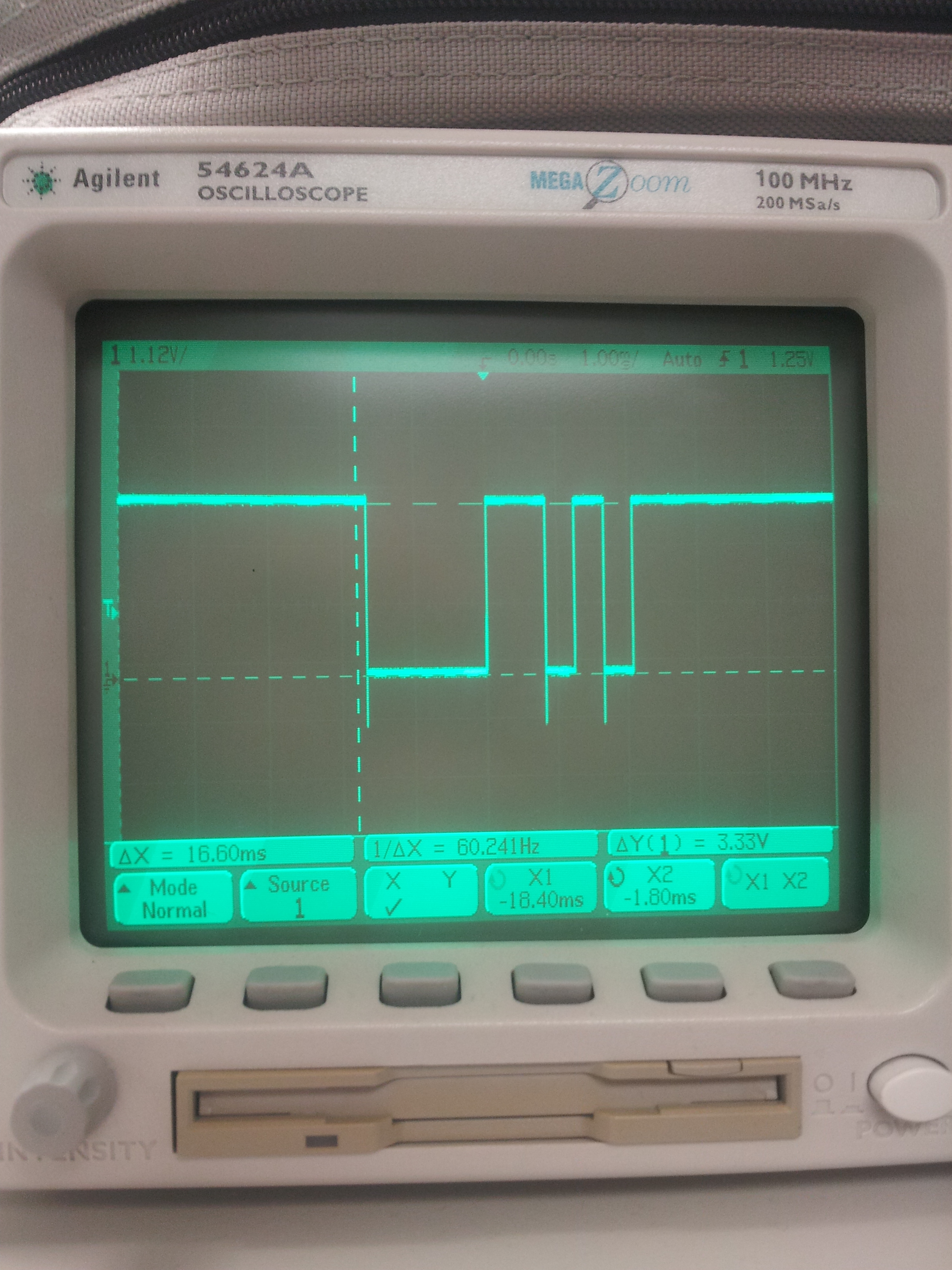
February 16, 2012 (5 hours):
Obtained the 10uF capacitor needed for the Vcap/Vddcore pin to allow the internal
voltage regulator on the micro to convert the 3.3V Vdd to 2.5V for the microcontroller core. Obtained an RJ-11 cable from Chuck for use with
the ICD 2 debugger, stripped the wires on one end, and soldered headers to the wires for use with the microcontroller breakout board. Applied
initial power to the microcontroller breakout board, and was able to successfully connect to and program the micro via the MPLAB software. Created
an initial hearbeat program using one of the timer modules and an interrupt, which toggles an I/O pin when the timer count reaches 0xFFFF.
Since the peripheral clock for the microcontroller currently operates at 4MHz, the square wave generated should have a frequency of
4M / 2^16 / 2 ~= 30.5 Hz This result was successfully observed on an oscilloscope, as shown below.
PIC24 Breakout Board 2/16/12 (With ICD 2 debug interface):
.jpg)
Square wave heartbeat program:
.jpg)
February 18, 2012 (2 hours):
Met with Jeff to begin testing the newly obtained FT232 breakout board
from Sparkfun. The goal for tonight was to be able transmit a single character from one of the UART modules on the microcontroller to the FT232, which would then
transmit the character via USB to a virtual COM port on a PC. Initialized the UART1 module to 9600 baud, 8 bit data, no parity, and 1 stop bit. Placed a character
in the UART1 transmit buffer, but was unable to retrieve the character on the PC side. Connected an oscilloscope to the Rx pin on the FT232, and could see that the character
was correctly transmitted by the UART module, but would still not show up on the PC terminal.
Scope signal of UART1 character to FT232:
WEEK 06 SUMMARY
Accomplishments: Verified how several peripherals would interface with the microcontroller. Successfully constructed a breakout
board for the PIC24FJ256GA106, and created an initial "Hello World" heartbeat program to verify functionality. Began to interface with the
FT232 module, but were unable to receive a character on the PC side.
Weekly Work Total: 13 hours
Project Work Total: 60 hours
February 19, 2012 (3 hours):
Continued working on interfacing with the FT232 module, with the goal of receiving a character on the PC
side sent from the UART1 module on the microcontroller. Soon found out that characters could be received on the PC via USB only when the power cord was connected
to the laptop that was being used for communication. As soon as the power cord was removed, communication would stop. Began to look into USB power specs for laptop
on battery vs. not on battery, but could not find any obvious solution to this strange problem. Wrote a basic function to transmit strings of data via UART, but soon found that
the printf function in the
February 20, 2012 (6 hours):
Fixed the problem with the FT232 only working when the power cord is attached to the laptop. Apparently,
not all of the ground rails on the breadboard were connected together, and this was causing unpredictable behavior with the FT232 module. Began to create another
test program using both the UART1 and UART2 modules of the microcontroller, with the goal of sending a character from the PC to the Rx pin of UART2 via
the FT232 chip, then copying the character from the UART2 Rx buffer to the UART1 Tx buffer, and sending it back to the PC via UART1 and the FT232 chip. Ran into
a whole bunch of weird issues, where only one UART module or the other would work at a time. After a lot of debugging, it was discovered that the Peripheral Pin Select
registers, which controlled which pins were used for each peripheral module, were set by default to only allow one write sequence. Once this default setting was changed,
both UART modules were able to work at the same time, and the echo to terminal program proved to be successful. Another program was also created to read in data from
the RFID module via UART2, and verify the RFID code against a stored list of valid "keys". This program also proved to be successful.
February 21, 2012 (8 hours):
Connected the GPS module to a breadboard and was able to recognize the device by using the Trimble GPS Studio PC
program. Able to successfully configure the GPS device via the PC program, log messages, and convert the messages to ASCII text for further analysis. Unable to actually obtain
any sort of GPS lock or coordinate data at this time due to lack of an antenna for the GPS device.
Moved focus from the GPS to the digital compass module, which interfaces via I2C. Researched the I2C protocol to understand the fundamental communication pattern between
devices. Next, looked at the application notes and datasheet for the compass, to understand which registers to initialize for functionality. Began initializing the I2C1
module on the microcontroller for 100 KHz (standard mode), and creating routines to send and receive bytes to both the accelerometer (slave address 0x18) and the magnetometer
(slave address 0x1E). After initializing I2C module and creating functions for communication, a test program was developed to retrieve accelerometer data and display it to the PC
terminal. Programmed the micro and ran test code, but unable to retrieve data from the compass module. Placed a scope on the I2C lines, but did not see logic signals being transmitted.
Further debugging will be necessary.
February 22, 2012 (3 hours):
Verified pins on microcontroller schematic to ensure correct PCB connections. Only the I2C lines and all Vcc/Vdd pins are
required to be connected to very specific pins. All UART and SPI pins can be assigned to any RPx pin (reprogrammable peripheral pins) on the device, and any GPIO pins can be
assigned to any Ryx pin, where 'y' is an I/O port letter, and 'x' is a corresponding pin number for that port.
February 23, 2012 (4 hours):
Focused on the compass and I2C module again. Suprisingly, after reconnecting the compass module to the micro, the I2C module
worked immediately. Created a test program to obtain both accelerometer and magnetometer data, and display to the PC terminal (picture below). Partway through the night,
the I2C stopped working and began displaying behavior similar to what was seen on Tuesday. After some tinkering with wires and reprogramming the micro, the module began working
again with no actual changes in software. Could not replicate the problem again for the rest of the night. Not sure if this is a software or hardware problem yet, but leaning towards
the hardware side.
Accelerometer and Magnetometer Data:
.jpg)
WEEK 07 SUMMARY
Accomplishments: Able to communicate with PC via UART1 module, and RFID via UART2 module. Able to communicate with GPS via PC application. Able to
obtain accelerometer and magnetometer data via I2C1 module, but errors may still exist either in hardware or software.
Weekly Work Total: 24 hours
Project Work Total: 84 hours
February 27, 2012 (3 hours):
Shifted focus from software development to preparation for the upcoming Design Review on
Wednesday. Created two powerpoint slides related to the preliminary software design and development status. Some of the software accomplishments thus
far involve communicating with the FT232 module via UART1, receiving RFID data via UART2, and communication with the compass module via I2C. The next
goals on the software side of things are initilizing communication with the GPS module (UART3), LCD screen (GPIO), and MicroSD card (SPI). Also created
a small table catagorizing the pins used on the microcontroller into pins used for initial setup (Vcc/Vss/Debug/MCLR), pins used for serial communication
(UART, SPI, I2C), GPIO pins for the LCD and pushbutton, and PWM pins for the speaker and servo. As of now, 13 pins are used for initial setup, 13 for serial
communication, 15 for GPIO, and 2 for PWM. Altogether 43 of the 64 pins are currently in use. Began working on Component Selection slides, which will
be heavily based off of the ones used for the Design Constraint presentation.
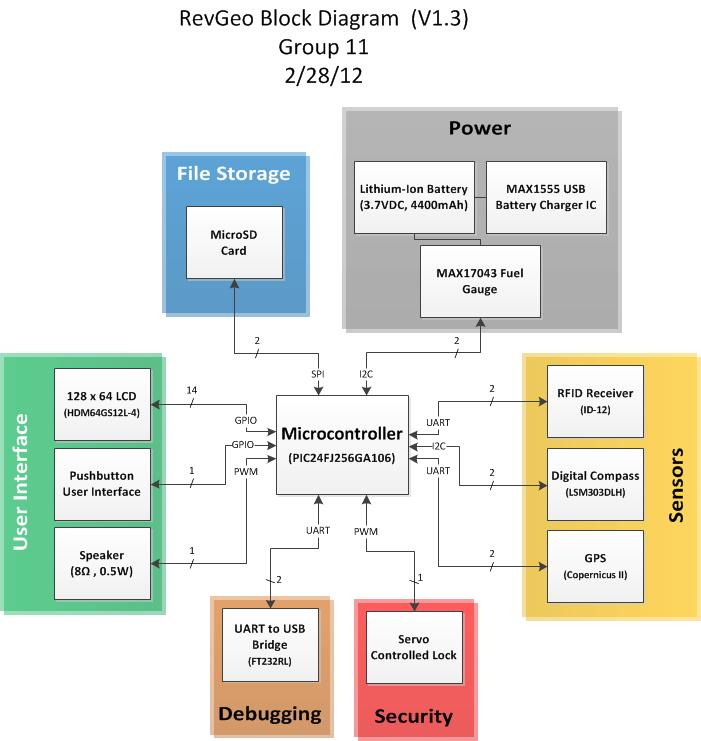
February 28, 2012 (4 hours):
Completed the Component Selection slides for the Design Review tomorrow. The major component choices
that will be discussed include the PIC24FJ256GA106 microcontroller, Trimble Copernicus II GPS Receiver, LSM303DLH Digital Compass, and ID-12 RFID receiver.
Updated the block diagram for the project, removing the LEDs for user interface, and added the MAX17043 Fuel Gauge to monitor battery status. The LEDs were removed
as the team believes the compass heading would be able to be displayed using the LCD screen instead, which would simplify the PCB design and also help to reduce
power consumption for the project. Worked with Jeff to finish up the Schematic and Theory of Operation slides, and polished up the entire Powerpoint document for
the presentation tomorrow.
System Diagram v1.3:
March 3, 2012 (2 hours):
Worked with Jeff to re-connect the GPS module to the Trimble GPS application on the PC. The
FT232 breakout board is used to provide a serial to USB conversion, so that the device can be recognized through a virtual COM port on the PC. Connected
the newly obtained antenna to the GPS and applied power. The PC application was able to show the connection status of each satellite detected, and by moving
the antenna to a window, enough satellites were discovered to start obtaining position data. The next step was to take the GPS unit (complete with breadboard)
outdoors and test tracking while moving. The GPS was placed inside of the Pelican case, and the lid was placed on top to simulate normal operation. A route was
walked, and then promptly repeated, since both teammates forgot to enable logging of data on the PC the first time. The data results were highly accurate, as
shown in the image below (The team attempted to spell out "HI" near the bell tower), but the GPS had some problems initially discovering the satellites in between
the first and second runs. More experimentation is required to determine if this was related to the positioning of the GPS, or some other factor.
GPS Tracking, Logging, and Mapping via PC:
.jpg)
WEEK 08 SUMMARY
Accomplishments: Prepared all required materials for the Design Review presentation, and performed initial satellite acquisition
of the GPS module, in addition to logging and mapping data via the Trimble PC application
Weekly Work Total: 9 hours
Project Work Total: 93 hours
March 4, 2012 (3 hours):
Created a detailed Excel document regarding pin assignments for the PIC24FJ256GA106.
This spreadsheet includes a list of all pin numbers, all possible uses for each pin, whether or not the pin is 5V input tolerant, the chosen
functionality of each pin for this project, the associated peripheral for each pin, and any special notes for each pin. This will help greatly
in the upcoming week, since the pin assignments will most likely need to be shifted around before the PCB is finalized. Discussed proposed
changes to the PCB with the rest of the team. Most likely, the GPIO pins for the LCD will be moved so that all of them correspond to pins on Port B,
rather than scattered around Ports G, B, and F. Also, headers and traces might be added to the PCB to allow the second serial port on the
GPS to be used in combination with an additional (removable) FT232 module for easy programming, logging, and mapping of GPS data for debugging purposes,
even when connected to the PCB.
Detailed pin mapping for microcontroller:
.jpg)
March 5, 2012 (3 hours):
Shifted focus to the MicroSD card and the Microchip Memory Disk Drive Library with the goal
of being able to successfully read and write to files on the MicroSD card before the PCB is sent out for fabrication. Started looking at the
files in the library used for the MDD/SPI interface. The FSIO.c/FSIO.h files deal with the high level file system management operations, including
reading and managing the File Allocation Table for the MicroSD card file system, managing read/write handles for files, and file creation and deletion.
The SD-SPI.c/SD-SPI.h files deal with the lower level SPI specific fuctions for sending and recieving data to the MicroSD card. Another important file
is HardwareProfile.h, which contains microcontroller specific information such as the names of the SPI control registers, pin assignments for the
SPI related pins, and clock speed of the microcontroller. The values in this file will need to be modified to correspond to the pins and registers
chosen on the PIC24FJ256GA106 microcontroller.
A new LCD was ordered today as well, as the current LCD is unable to output a negative voltage on its Vee pin, which is required for the LCD contrast.
The new LCD is the GDM12864HLCM, which has the same parallel interface as the previous choice.
Hopefully, the previous LCD was defective, and this LCD is able to correctly output a negative voltage on Vee.
March 6, 2012 (9 hours):
Started to look at the HardwareProfile.h file for the Memory Disk Drive File System Library.
Defined the control registers used for the SPI1 module, as well as the pins used for SDI, SDO, SCK, SD_CS (chip select), and SD_CD (card detect).
Also defined the system clock frequency, and removed initialization of the SD_WE (write enable) pin, since write protection of the MicroSD card
will not be checked in this implementation. Modified the MDD_SDSPI_InitIO and MDD_SDSPI_WriteProtectState functions in SD-SPI.c to reflect the
absence of the SD_WE pin. Added the connection for the SD_CD pin to the project schematic, as it was previously unincluded. This pin allows the
microcontroller to determine if and when a MicroSD card is inserted into the MicroSD housing on the PCB. Finally, the reprogramable peripheral
pins (RP pins) were configured for the SPI module, code was added to main.c to test initial write functionality, and the code was programmed onto
the microcontroller. The microcontroller was able to successfully write data to AND read data from the MicroSD card without any issues.
Worked with Paul and Jeff to completely remap the microcontroller pins for this project. Using the detailed Excel document created on Sunday, most
of the pins were shuffled around so that they would fit better on the PCB layout. The 8 pins used for LCD data now correspond to Port B pins RB8-RB15,
and the 6 pins used for LCD control signals correspond to Port E pins RE0-RE5. All of the serial communcation pins were broken out to headers to ease
in debugging the PCB. Finally, several currently unused pins were also broken out to header pins to allow for any unforseen changes once the PCB has
been fabricated. These pins include additional reprogrammable peripheral (RP) pins, additional GPIO pins, and the third I2C module pins.
March 8, 2012 (2 hours):
Finalized everything needed for the Proof of Parts homework assignment and PCB layout.
The team demonstrated the Proof of Parts to the TA, and was checked off for completion. A FreeDFM check was performed on the PCB, and no
major errors were found. Paul will submit the final PCB schematic tomorrow morning.
WEEK 09 SUMMARY
Accomplishments: Successfully able to write and read to a MicroSD card via the SPI interface. Completely remapped
microcontroller pins for easier hardware routing as well as software programming. Finalized the PCB, and submitted it for
fabrication
Weekly Work Total: 17 hours
Project Work Total: 110 hours
March 11, 2012 - March 17, 2012 (0 hours):
No senior design work was performed, as this week was Spring Break.
WEEK 10 SUMMARY
Accomplishments: None, Spring Break.
Weekly Work Total: 0 hours
Project Work Total: 110 hours
March 19, 2012 (7 hours):
Began looking at the LCD driver code to be used for this project. The basic driver was
written by Radoslaw Kwiecien, and contains many low level files to support a variety of different
microcontrollers. The driver for the PIC24 will be based off of the pre-existing KS0108-PIC16.c file, as the initializations required for the PIC24
will similarly resemble the ones for a PIC16. A few changes will be needed however, as the PIC16 has 8 bit "ports" while the PIC24 has 16 bit "ports".
Therefore, instead of directly writing and reading 8 bit data from a port, careful consideration must be taken to ensure the state of the other pins
not associated with the LCD are unaltered. Completed the required changes for LCD initialization, but will wait until tomorrow to test, since Jeff
has more experience wiring up the LCD and level converters. Worked on and completed a flowchart detailing the initialization and main loop operations
for the software application. Also, a code hierarchy was developed, showing that the main application will make calls to 8 different interfaces
(PC Debug, RFID, GPS, Compass, Fuel Gauge, MicroSD, LCD, and Miscellaneous).
Software Flowchart (initializations):
.jpg)
Software Flowchart (main loop):
.jpg)
March 20, 2012 (8 hours):
Worked with Jeff to verify functionality of the 3.3V to 5V level converter, then connected
the LCD through the level converter to the PIC24FJ256GA106 for initial testing. When the micro was released from reset, the LCD immediately displayed
"Hello World!" as planned. Further work was done to test displaying bitmaps to the LCD screen, which also proved to be successful. A large amount of
searching was performed to find a "clock-like" 32x32 pixel bitmap that could be used to display a graphical compass heading with a resolution of 30
degrees. A suitable animated .gif file was found, which was then converted into 12 individual .jpeg frames, then edited and finally converted
to 32x32 pixel bitmaps. These bitmap images were then combined into one 32x384 pixel image, and converted into an array of data in a header file by
using the LCD Assistant utility. These images were verified on the LCD screen, and should function
perfectly for the RevGeo graphical compass. Also finalized the software Powerpoint for the TCSP presentation tomorrow.
LCD "Hello World" Initialization:
.jpg)
LCD Compass 0 and 30 degree heading:
.jpg)
March 21, 2012 (5 hours):
Completed the Introduction and Software Design Considerations portions of the software
report due on Friday. A large amount of research was performed to fully understand the memory mapping on the PIC24FJ256GA106. The program
memory (Flash) has a 24-bit address space, while the data memory (RAM) has its own 16-bit address space. In order to read the Flash as data,
the upper half of the data memory address space can be mapped to a 32KB page of Flash, which is then accessible by using the corresponding data
memory address. See the "homeworks" section of the webpage for more information.
March 22, 2012 (5 hours):
Completed the Software Narrative portion of the software report, in addition to updating
and finalizing the reference list, appendices, and hotlinks to code snippets. A large amount of initializations for code modules has been completed,
and the next major steps in code development will be to communicate and receive data from the GPS unit, as well as calculate a compass heading
from the raw accelerometer and magnetometer data that has been obtained.
WEEK 11 SUMMARY
Accomplishments: Completed LCD initialization and display code. Completed and submitted Software Narritive
homework assignment.
Weekly Work Total: 25 hours
Project Work Total: 135 hours
March 26, 2012 (2 hours):
Began looking at the
application notes for calculating a compass heading with tilt compensation, as well as the steps required to calibrate both the accelerometer
and magnetometer devices. The calibration method involves gathering raw data at predetermined orientations of the compass device, and using this
data to calculate the parameters used for the normalization of further compass measurements.
Example code was also found for the heading calculations with tilt compensation, and efforts will be made to adapt this code to the
PIC24FJ256GA106 tomorrow.
March 27, 2012 (5 hours):
Re-organized the code for the compass module to create 3 main interface calls: Compass_Init(),
which initializes the microcontroller pins and configures the registers on the compass device, Compass_GetData(), which obtains the raw data from the
compass module, and Compass_CalcHeading(), which calculates the compass heading with tilt compensation. The example code found yesterday was modified
to work with the PIC24 microcontroller, and the test program was able to successfully calculate a heading and display it to the PC. Accuracy of this
calculation has yet to be verified, and the calibration sequence for the compass has not yet been performed.
Compass heading calculation:
.jpg)
March 28, 2012 (5 hours):
Began looking at how to calculate the distance between two pairs of GPS coordinates, as well as
calculating the initial heading in degrees. A website was found that explains these
calculations in great detail. These equations will be used once GPS data has been obtained from the GPS receiver. The decision to store the
MicroSD card route data to flash was re-evaluated, and will no longer be implemented as writes to flash must be done in blocks of 192 bytes, and
erase operations must be done in blocks of 1536 bytes. These sizes would prove to be a huge inconvenience, especially since the flash would
need to be continuously updated to reflect the completion of each waypoint. The new solution is to store the total number of waypoints and the
number of waypoints completed as the first few bytes in the file on the MicroSD card. As waypoints are completed, the waypoint completed count on
the MicroSD card file will be updated, allowing for a non-volatile storage method that is much easier to implement than the on-chip flash.
March 30, 2012 (2 hours):
Worked with Jeff to solder the basic capacitors and resistors onto the PCB that are required
for initial communication with the PIC24 microcontroller. Tested the 3.3V and 5V supply rails on the PCB with a 3.7V input voltage from a power
supply and found that both rails were operating at the correct voltage levels. The goal for tomorrow will be to add the microcontroller to the PCB
and test an initial heartbeat program.
March 31, 2012 (5 hours):
Worked on merging test code modules into one single RevGeo1.0 build while Jeff soldered the
microcontroller and reset pushbutton to the PCB. Communication between the MPLAB IDE and the PCB microcontroller was then tested, and an initial
heartbeat program was loaded onto the microcontroller to toggle an LED on the PCB. The heartbeat program was fully functional, as shown in the image
below. Focus was then shifted to determining the format for route data on the MicroSD card. The plan is to have an exact number of bytes for each
piece of route data, so that it can be easily read from the MicroSD into SRAM. The format of the route data file is as follows: 2 bytes to store the
total number of waypoints in the route, 2 bytes to store the number of waypoints completed so far, 11 bytes to store each waypoint latitude, 11
bytes to store each waypoint longitude, and 20 bytes to store the text description of each waypoint. A test route file was created with 3 waypoints
in it, and code was generated to read each waypoint off of the MicroSD card and store each in SRAM. The test code proved to be successful, as shown
in the image below.
PCB heartbeat LED:
.jpg)
Route data read from MicroSD card:
.jpg)
WEEK 12 SUMMARY
Accomplishments: Microcontroller heartbeat program functional on PCB, Compass heading calculation with tilt compensation
successfully performed, route data read from MicroSD card and stored to microcontroller SRAM, GPS coordinate distance calculations
researched.
Weekly Work Total: 19 hours
Project Work Total: 154 hours
April 2, 2012 (6 hours):
Continued working on the MicroSD interface code by developing a function to update the route
data on the MicroSD card each time a waypoint has been reached. The function opens the file on the MicroSD card in "append" mode, seeks to the
correct position in the file, and overwrites the bytes containing the number of waypoints completed with the updated waypoint count. The function
then checks to see if the number of waypoints completed matches the total number of waypoints, and notifies the calling function if the route
is now complete. Also added code for calculating the distance between GPS coordinates, as well as initial bearing. Verified functionality of
these functions using several pairs of GPS coordinates, and the results proved to be very accurate. Verified functionality of the FT232 USB to
UART bridge on the PCB once Jeff finished soldering all of the components on the board. Lastly, #ifdefs were added to the code to account for the
different initializations between the PCB and experimental board. By defining PCB_BUILD, the I/O pins for the micro are correctly initialized to
match the traces on the PCB.
FT232 working on PCB:
.jpg)
GPS distance and bearing:
.jpg)
April 3, 2012 (8 hours):
Verified functionality of both the RFID and Compass modules after all of the components were
soldered onto the PCB. Began working with Jeff to figure out the communication protocol to be used with the GPS. It was determined that the
Trimble TAIP protocol would be used, as the protocol uses plain ASCII text strings to send information to and from the GPS. Used the Trimble
Studio PC application to configure the GPS to output the PV (Position/Velocity) command once every second. The PV command contains the current
longitude and latitude, current velocity and time, and additional bytes to indicate whether or not the data is current/old/invalid. Created the
microcontroller code to read and parse the PV messages recieved from the GPS to extract the GPS coordinates to be used in the distance and bearing
calculations. The GPS code will be tested on the microcontroller and PCB tomorrow.
April 4, 2012 (9 hours):
Tested the GPS module on the PCB with the microcontroller code written yesterday. The micro is
able to successfully parse the message strings received from the GPS, and is able to extract the latitude and longitude values once the GPS has
achieved satellite lock. The next goal was to verify the MicroSD card functionality on the PCB. This proved to be extremely challenging. While
the code worked flawlessly on the experimental board, the micro on the PCB was unable to identify/read anything. Upon closer inspection of the
PCB schematic, it was discovered that a few of the traces for the MicroSD card were laid out incorrectly. After carving away some traces and
fly-wiring a new solution, the micro was still unable to read from the card. Several hours were spend trying to debug the issue, but no progress was
made. Finally, several spare broken-out pins on the micro were connected to a breadboarded MicroSD solution, and communication was finally made. It
is unknown if the issue with the MicroSD on the PCB is related to the MicroSD housing/soldering connections, PCB traces, microcontroller pins, or
even software initializations. More research will be needed to discover the issue. A late night test of the GPS and breadboarded MicroSD card
was conducted around campus, using a route of 3 GPS coordinates. The testing proved to be extremely successful, as shown below.
Late night route test Part 1:
.jpg)
Late night route test Part 2:
.jpg)
April 5, 2012 (3 hours):
Added the LCD code to the RevGeo1.0 build, and tested LCD functionality on the PCB. The LCD
does not display correctly when connected to the PCB, even though it is fully functional on the experimental board. The team has begun to suspect that there is an issue with the micro
currently soldered to the PCB that is affecting both the MicroSD card connections and the LCD. The microcontroller will on the PCB will be replaced
tomorrow to see if any of the problems are fixed.
April 6, 2012 (1 hour):
Jeff replaced the microcontroller on the PCB and the MicroSD card and LCD were re-tested.
Unfortunately, both problems still exist. While this eliminates the faulty micro hypothesis, there are still several possible reasons for the
two components not functioning properly. Major hardware/software debugging will be needed to solve these two issues.
WEEK 13 SUMMARY
Accomplishments: GPS, RFID, compass, and USB to UART bridge work on the PCB. MicroSD card works only when using spare
micro pins and breadboarded connections, and LCD is not yet functional on the PCB. Most all of the code modules are complete,
with just main loop code left to bring all of the functionality together.
Weekly Work Total: 27 hours
Project Work Total: 181 hours
April 9, 2012 (3 hours):
Focused on fixing the issues with the LCD and MicroSD card on the PCB. Jeff closely inspected
the pins on the 3.3V to 5V level converter chip going from the micro to the LCD and found that a bit of excess solder was tying two of the pins
together. Once he removed this excess solder, the LCD began functioning properly on the PCB. Experimented with various combinations of pins for
the MicroSD card, using different combinations of the orignal pins and the extra broken out pins. It was found that the SCLK, MOSI, and Chip Select
pins worked on both the original and broken out versions, but when two out of the three were on the original pins, a faint, high pitched sound
would come from the PCB. The other two pins, MISO and Card Detect would only work on the broken out pins. Unable to discover a consistent solution
after a few hours of work, the team decided to just fly-wire the five broken out pins to the MicroSD card, and use all of those instead of the original
pins. This fixed the issue, and the MicroSD card was fully functional on the PCB.
Fly-wired MicroSD solution:
.jpg)
April 10, 2012 (3 hours):
Added code for both the buzzer and the servo. Both devices use PWM signals, which are
created using Output Compare (OC) channels on the micro. OC1 was initialized to output a 50% duty cycle square wave at 2.4KHz for the buzzer, and
OC2 was initialized to output a 3% to 8% duty cycle at 50Hz for the servo. Also added a 1/4 sec. timer to be started when the buzzer is turned on,
and automatically turns off the buzzer when it expires. Buzzer functionality was tested and confirmed. Servo functionality was then tested, and
an issue was discovered. Each time the servo was turned on, the output of the FT232 to the PC seemed sporadic and repetative. This behavior
seems to point to the microcontroller resetting uncontrollably when the servo is turned on, most likely due to the servo drawing more current
than the voltage converters can supply. A solution to this issue has not yet been determined.
Servo causing micro resets:
.jpg)
April 11, 2012 (7 hours):
Worked on creating the layouts for the screens to be displayed on the LCD. An initial
startup screen will welcome the user, and wait for GPS lock. Once GPS lock has been obtained, the screen will display the current waypoint
count, a text description of the next waypoint location, the distance to the next waypoint, both the desired bearing and current bearing, and
a graphical "arrow" pointing in the direction on the next waypoint. Another screen will be used to display when the box has been unlocked by
an RFID master override, and a final screen will be used to display when the box has been unlocked after all waypoints have been visited. Added
main loop code for the first two screens, and brought the device outside for testing. The startup screen worked, but the main screen displayed
garbage. After removing the graphical "arrow" from the main screen (the suspected culprit), the main screen displayed, but the desired bearing
was stuck at zero, and the screen would have small glitches when updating on occasion. After fixing the desired bearing code and creating a
longer delay when strobing the LCD, the two issues were fixed. The graphical "arrow" will be looked at tomorrow to find a solution.
LCD main screen:
.jpg)
April 12, 2012 (8 hours):
Fixed the graphical "arrow" display on the LCD, but the compass heading determined by
the accelerometer and magnetometer measurements seems to be inaccurate. Calibration and compensation for existing magnetic fields might need
to be done at a later time. Added main loop code for locked and unlocked states of the box. Also added functions in the code to turn off
the UART modules and timers used for the RFID, GPS, and Compass once the box is unlocked, since the flags will not be serviced once the box is
in an unlocked state. Additional functions were then created to re-enable these modules when the box is re-locked. Another function was created
to "reset" the current route when re-locking the box. This routine checks to see if a new route was put on the MicroSD card when the box was
open. If a new route was created, the micro reads this new route and begins operation. If the old, completed route still exists, the number
of completed waypoints on the MicroSD card is overwritten to zero, and the route is re-read into RAM. Tested functionality of all locked and
unlocked states of the box as well as all LCD screens, which proved to be successful.
April 13, 2012 (3 hours):
Focused on fixing a persistent issue experienced when first applying power to the PCB. Each
time power is applied, the oscillator settings do not correctly engage on the microcontroller. This causes incorrect baud rate settings, and
basically results in the PCB being non-functional. The issue is fixed, however when the reset button is pressed, pulling the MCLR pin low and
causing the micro to restart. Since applying power, and manually pressing a reset button each time the device is turned on is not a desired solution
a few lines were added in software to initially check the oscillator settings, and cause a software reset if incorrect. This seemed to fix the
issue. An email was sent to Microchip to see if they have a better solution than generating a software reset, since the oscillator settings
should correctly engage the first time under normal operating conditions. Also tweaked the PWM duty cycles for the servo based on values provided
by Jeff. The issue with the servo causing resetting of the micro was solved by using 4 AA batteries as a separate 6V power supply instead of
pulling off the 5V supply used for the RFID and LCD.
WEEK 14 SUMMARY
Accomplishments: Issues with LCD and MicroSD fixed for the PCB. Buzzer and servo code added and functional. LCD
display screens created and functional. Main loop code updated to reflect locked/unlocked states. Oscillator problem
fixed.
Weekly Work Total: 24 hours
Project Work Total: 205 hours
April 15, 2012 (2 hours):
Performed testing of the RevGeo box with all components inside of the enclosure. Testing
proved to be extremely successful, but as stated last week, the compass calculations were still inaccurate. A new, larger
antenna was used for these tests, and was able to acquire GPS lock much faster than the
smaller antenna that was used previously. This new antenna will be included in the final RevGeo design. With most of the packaging now complete
for the design, 4 out of the 5 final PSSCs should be able to be demonstrated tomorrow.
RevGeo Packaging (Outside):
.jpg)
RevGeo Packaging (Inside):
.jpg)
April 16, 2012 (3 hours):
Demoed the RevGeo to the TA and got 4 out of 5 final PSSCs checked off. The main focus is
now on improving the accuracy of the digital compass. Found some example code
detailing a calibration method for the magnetometer, which involves rotating the device on all axes, and recording the maximum and minimum values
measured in the x, y, and z directions. These values are then hard-coded into the application, and used to shift and scale all further magnetometer
readings. In addition, the method of calculating the compass heading was modified to more closely resemble that of the new example code. After
calibration was performed, the new code was tested out and proved to dramatically increase the accuracy of the compass. The final PSSC will be able
to be demoed tomorrow to the TA.
April 17, 2012 (1 hour):
Demoed the final PSSC to the TA on duty. All 5 PSSCs are now complete. A few things that
still need to be worked on include: Adding the pushbutton for locking the RevGeo to the enclosure, debouncing the pushbutton switch, and creating
more graphical images for the Welcome splash screen and the route complete screen on the LCD.
All PSSCs Complete:
.jpg)
April 19, 2012 (6 hours):
Paul created a RevGeo logo, which he then converted into a 128x64 pixel monochrome bitmap
image. This image was then converted into a header file using the LCD Assistant utility,
the same program used to create the graphical "arrow" for the compass. This image will be used for the Welcome "splash screen" displayed on device
power-up until GPS lock has occured. Another "Congrats" image was created and coverted to a header file to display when the route has been completed.
Jeff also added a red pushbutton to the top of the box to lock the device after a route has been completed. The rest of the night was spent
working on the User Manual, with emphasis on the Setup and Operating Instructions, and Troubleshooting Table.
Welcome Splash Screen:
.jpg)
Route Complete Screen:
.jpg)
April 21, 2012 (1 hour):
Added code to de-bounce the pushbutton using a 1ms timer interrupt. This code was tested
and proved to be functional. Brainstormed ideas for the PSSC video, which will be worked on tomorrow.
WEEK 15 SUMMARY
Accomplishments: Fixed compass issues with calibration routine, checked off all 5 PSSCs, added bitmap images to
the LCD, and completed the User Manual assignment.
Weekly Work Total: 13 hours
Project Work Total: 218 hours
April 22, 2012 (2 hours):
Worked with Jeff to record the raw footage for the PSSC demonstration video. The video
will consist of a brief introduction of the design and the components involved. Next, the process of creating a route in a .txt file, and
storing it on the MicroSD will be covered. Finally, the video will include an outdoor demonstration of a route being completed.
April 25, 2012 (0 hours):
Jeff completed the
PSSC demonstration video.
April 26, 2012 (4 hours):
Completed the individual contributions portion of the Final Report, focusing on contributions
related to the creation and debugging of all software modules both on the breakout board and PCB, as well as integration of all modules into
the final application. Provided support/advice to the current issue faced with the battery charging circuit, which causes the microcontroller
to run when the USB cable is connected to the PC, even when the power switch is turned off. This seems to be due to a common ground line problem
on the PCB, and would require some cutting of traces and fly-wiring to fix. Since this issue is not directly related to any of the team's PSSCs,
it may be left un-fixed in the interest of time.
April 27, 2012 (2 hours):
Revised Homeworks 3 and 9 for inclusion in the Final Report. Many changes were made to
Homework 9 to reflect the finalized code hierarchy used in the RevGeo design. See the Final Report for more details.
April 28, 2012 (3 hours):
Updated both the initialization and main loop flowcharts for the RevGeo application, as well
as the code hierarchy diagrams. All code modules in the code hierarchy are now complete, and the RevGeo application is fully functional. Completed
the "Version 2 Changes" section of the Final Report, detailing changes that would be made if the team build a newer version of the RevGeo. Some
changes include: moving the MicroSD and RJ11 jack on the PCB away from the servo, using a 5V step-up converter that could source up to 1A of current,
eliminating breakout boards from the final design, and creating a more robust user interface with another pushbutton and rotary pulse generator.
April 29, 2012 (6 hours):
Merged all homeworks into final report, and ensured all sections are uniformly formatted.
Final tweaks will be made to the report tomorrow before submission, but on the whole, the report is finished.
WEEK 16 SUMMARY
Accomplishments: Completed all final reports as well as the PSSC demonstration video. The RevGeo project is now
complete.
Weekly Work Total: 17 hours
Project Work Total: 235 hours