Tejas Kulkarni's Lab Notebook
Week 01
August 15, 2010 (2 hours):
Met as a team after class to finish writing preliminary project proposal.
January 17, 2010 (2 hour):
Brained stormed the possibilities of developing a multi-touch table. The Multi-touch table would require an external camera as an interface for the Computer Vision Algoithm. I researched that algorithms that fall under Image processing and Computer Vision such as blob tracking and real-time contour tracing can be used to track fingers on the multi-touch surface. After studying the feasibility of the project, I was positive that the project would work and would be promising.
WEEK 01 SUMMARY
Accomplishments: Submitted preliminary project proposal.
Weekly Work Total: 4 hours
Project Work Total: 4 hours
Week 02
January 19, 2010 (2 hours):
Met as a team to formulate PSSC for presentation in class on September 2.
January 20, 2010 (1 hours):
I worked on the class PSSC1 presentation. I also worked on laying out the rought draft of our PSSC's.
January 21, 2010 (7 hours):
Met as a team to finish the final project proposal.
Met with Chuck and got the Intel Atom board. The Intel Atom board was packaged in a black box. Me and Abhisheyk will try to install Windows Embedded XP SP2. I also personally researched the main difference between Windows Embedded XP and normal XP Professional edition. This is important because we want to know whether we can use service packs such as Microsoft Visual Studio 2008, OpenCV and other Computer Vision libraries. From what I researched, the Embedded XP differs in the following ways :
1. Embedded XP does not support Windows File Protection (WFP). WFP prevents system files from being overwritten unless the files that are being installed are digitally signed by Microsoft. We do not require this feature to implement the hand tracking feature in C++/OpenCV
2. Embedded XP does not support XP tour (which is useless anyways)
3. Embedded XP does not support the feature to Add/Remove programs option in the Control Panel
4. Embedded XP also does not have online activation. This is fine since we are going to obtained that while downloading XP on the Atom board
5. Embedded XP does not support Windows Update, Image Acquisition file and MSN Explorer. We can live without it for sure.
Taking into account my research, I concluded that we can safely proceed with whatever we were going to do with Intel Atom
January 23, 2010 (5 hours):
I worked on getting the camera to work with our proposed design. The camera in use had to support IR filtering. We have a PS3 eye camera. This camera is the one usually used by gamers to play PS3 bsed online games. This camera is of high resolution with the following specs -
1) 680x450 pixel resolution
2) Wider angle for viewing and
3) 30 fps
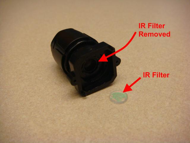
The high resolution precisely tracks the finger blobs effectively.The high frame per second will ensure that we will have a good chance to perfect our blob detection. I basically hacked into the Ps3 eye to facilitate IR based tracking. To do this, I removed the IR filter from the PS3 eye. This was the first attempt and it had to fail. I am ordering another PS3 eye camera to play around with. Hopefully this one won't break.
WEEK 02 SUMMARY
Accomplishments: PSSC and project proposal finalized. Worked on getting the Sony PS3 eye camera to work with our system (not working properly yet). Installed Win XP and setup of other vital features on the Intel Atom board. Evaluated Embedded Win XP to implement the Image Processing part
Weekly Work Total: 15 hours
Project Work Total: 19 hours
Week 03
Jan 26, 2010 (8 hours):
I met with Abhisheyk to to mainly work on developing the top level framework for the Computer Vision based algrithms and its relationship with the Graphical User interface we were about to build in the weeks to come. I researched over some of the haar classifiers in the Computer Vision literature to get a feel of Image Processing and Vision systems. I looked up another algorithm namely the Lucas Kanade algorithm to get a feel for tracking algorithms.
We have decided to exchange information between the Vision module and the GUI interface via the TUIO interface. TUIO interface was developed specifically to optimally transfer information related to blob tracking in Multi0-touch applications since the advent of the technology. TUIOis a communication protocol built to lead with multitouch technology, using OSC protocol to work. it is one of the most important elements in this kind of project, because it allows you to build multitouch applications using several kinds of technologies. TUIO sends the funger tracking data on a server on port 3333. The client application (anything ranging from Java, Processing, Flash etc) can read onto this port and use the data for constructing the user interface. This is an illustration :

I also researched about the techniques to accomplish Total Internal Reflection on the touch table surface. This is important because the camera can see only the points where the total internal reflection breaks on the surface. So for example, when a user touches on the table-top, the total internal reflection on the surface would break at that point and the camera sees a "blob" due to this phenomenon.
Later in the night, I struggled for a couple of hours on trying to install OpenCV along with the OpenFrameworks. After a lot of frustration, I figured out that the Embedded Win XP Visual Studio lacked the following DLL files : MSVCP17.dll and MSVCR1.dll. Error was fixed and OpenCV/OpenFrameworks runs in the Visual Studio enviroment.
Jan 27, 2010 (3 hours):
I worked further on hacking into the PS3 eye camera. We want to make sure that we do not have to order another camera. This is sequence of operation I followed to remove the IR filter from the camera (Thanks to AlexP, alexp@lvcm.com):


Jan 28, 2010 (5 hours):
I met with Abhisheyk to buy Graphics LCD. We researched for quite a while before purchasing the OLED from 4D-Systems. The LCD has an in-built touchscreen module and the dimensions are 2.4" display. The OLED is ultra-thin and low power.
AS a team, we met with David and Prof. Mark Johnson to clarify and discuss about our PSSC's. We were later joined by Malek who gave us helpful advise about choosing an appropriate Bluetooth controller
Jan 29, 2010 (3 hours):
First, we met Malek to discuss about which microcontroller to use for our project. He suggested using Freescale over PIC and Atmel. We decided to use 9S12 Freescale for our project. Later in the afternoon, we charted our design (given in Presentations) to employ two Freescale microcontrollers to implement the design
WEEK 03 SUMMARY
Accomplishments: OpenCV and other Image Processing tools succesfully setup. TUIO and flosc successfully setup/initialized. Got the PS3 eye camera to finally work as per our requirements. Errors with the Visual Studio environment fixed. Decided upon using Freescale 9S12 microcontroller
Weekly Work Total: 19 hours
Project Work Total: 38 hours
Week 04
February 2, 2010 (6 hours):
Met with the entire team to complete the Design Constraint Analysis. I also researched way to "keep" the IR rays from escaping the plexiglass. Found a forum which had a tutorial to make a "silicon rubber" sheet on a blotting paper. This will hopefully leads towards a succesful Internal reflection.
February 4, 2010 (8 hours):
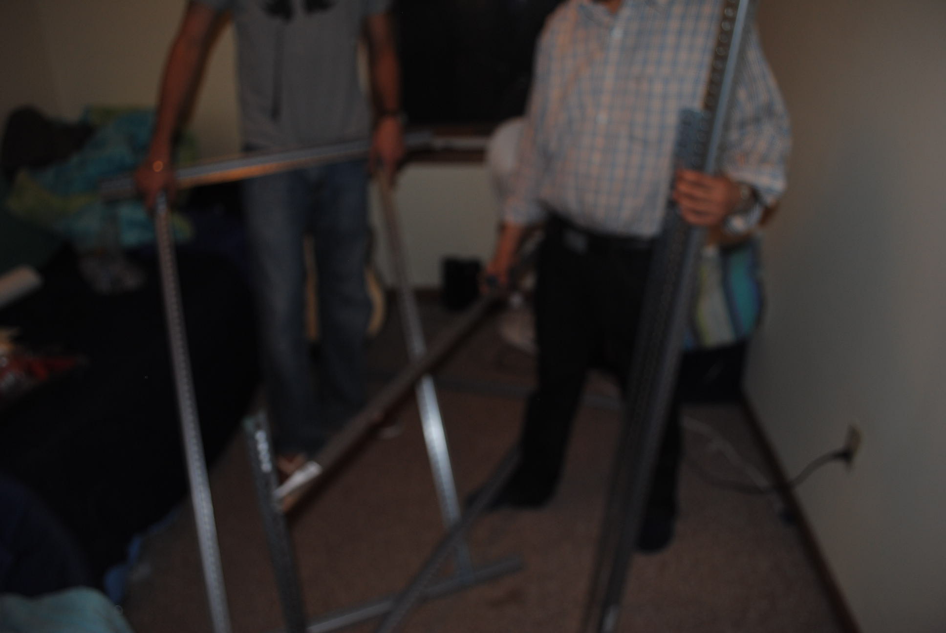
We had already obtained all the parts to constuct the table. We decided to make the table in my Apartment since the size is to big to fit in the Senior Design lab. Me and Abhisheyk had purchased the plexiglass, the metal rods and other hardware from Menards a few days ago. I also came to know that the total internal reflection would not break if we just keep the plexiglass as it is on the table. This is mainly because the glass allows the passsage of IR rays and thus there is no internal reflection. I had been looking into addressing this problem yesterday. Me and Abhisheyk went to Wallmart the other day to buy Silicone, Xynol and other essentials to make the magical "rubber sheet". A detailed description of how the table was constructed along with the installation of IR LED's and the "silicon rubber" sheet is as follows :
1. The first step was to construct the table using the metal joints and rods. After a few painful hours, we managed to hold the table on the ground. These are a few sample pictures I took in the process of developing the tabletop.


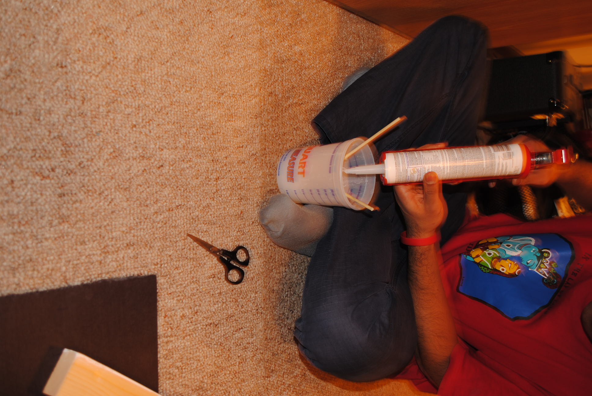
2. In between constructing the table, I started mixing up the ingredients to make the magical "silicon rubber" potion. We first used a plastic glass for the mixture, but it melted because of the combination of silicone and xylol. We got a painter's plastic jar to perform the mixing. A 1:1 ratio of Silicone and Xylol was stirred for about 15 minutes. A blotting paper was taped onto the wall. A painting brush was used to apply the mixture onto the blotting paper. Approximately three layers of this mixture was put on the paper. The procedure was completed after drying the paper for about 2 hours. These are some of the illustrated photos of the entire procedure :
This was used to apply the mixture onto the blotting paper:

This is the blotting paper taped onto the wall:

All the essentials to make the magical "silicone rubber":

Stirring the mixture for about 15 minutes for each layer:
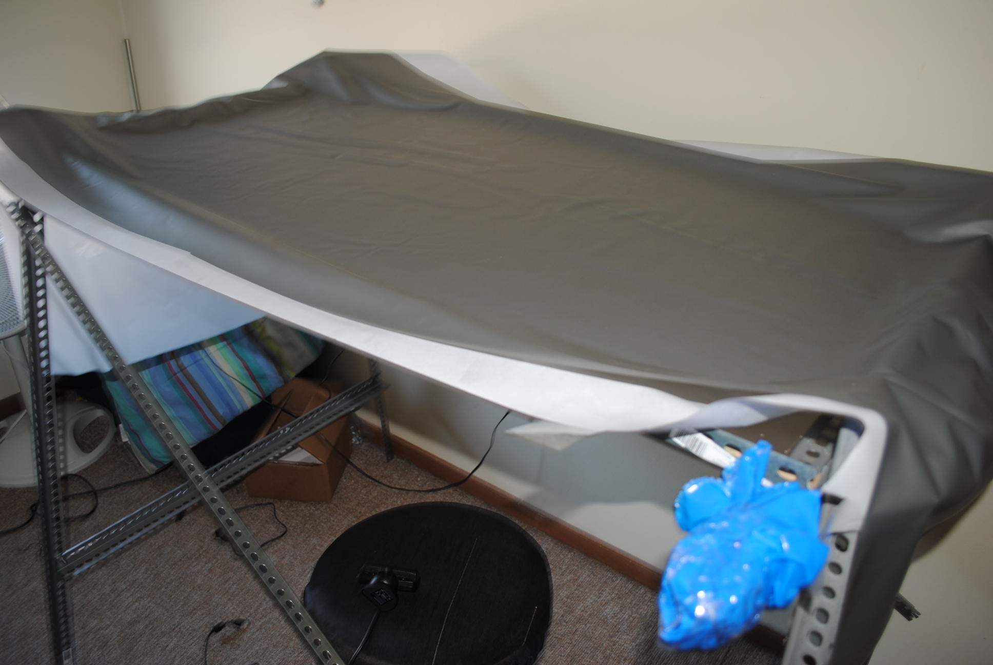
This is how the (technically) almost finished table looks (without any asthetics):
February 5, 2010 (2 hours):
Helped Himanshu complete the homework for that week
WEEK 04 SUMMARY
Accomplishments: Constructed a working Tabletop. Developed Silicone rubber sheet to allow Total Internal Reflection. Helped Himanshu in Presentation and Homework
Weekly Work Total: 16 hours
Project Work Total: 44 hours
Week 05
February 8, 2010 (7 hours):
I was experimenting with using Processing from MIT to use it as a GUI for our application. Processing is a computational art toolkit from MIT. It also supports OpenGL and a custom 3D Graphics API (P3D). Processing is natively written in Java but has its own development environment. Since we were going to write the USB drivers in Java, I ported Processing and added all the *.jar files of Processing in Java. I could compile Basic Processing code in a Java Applet. I also proceded to write a custom TUIO Port Listener. This small program recognizes finger activity on our table and draws it onto a Java Applet. This is a sample picture of the applet running:

Each finger blob has a unique Identifier. To develop a GUI app, my custom interface can act as an API to be called. The API would return the current blob on the table (via an ID number) along with the co-ordinates with respect to the resolution of the projector.
February 10, 2010 (5 hours):
I got the PIC24F development board from Chuck. I tried playing around with it. There were some library problems which were later on resolved. I tried going through the sample programming tutorial and running my first PIC program on the development board to display characters on the on-board LCD. Completed PADS tutorial
WEEK 05 SUMMARY
Accomplishments: Initial GUI development on the Intel Atom side. Started development tutorials on PIC24F dev board. Ran sample programs and developed an API in Processing for the Blob tracking mechanism and TUIO protocol.Completed PADS tutorial
Weekly Work Total: 12 hours
Project Work Total: 56 hours
Week 06
February 15, 2010 (2 hours):
Met with Abhisheyk and tried interfacing the OLED LCD with 9Sc12 microcontroller to see if it works. Development in progress...
February 16, 2010 (4 hours):
I worked on the TSSC presentation and the preiminary schematic. The preliminary schematic is nowhere close to what the circuit will look like. It is a mere depection of the top level diagram and a reference for what I will working on tomorrow
February 18, 2010 (10 hours):
I pretty much spent all day in the lab. Earlier I worked on talking to David about the issues we were getting into with the Bluetooth. Earlier that day, I talked to Chuck and tried searching for the problem without any luck. David helped in fixing the problem after he identified that the problem was the varying voltage levels in the SCI communications. All we had to do was stick the Rx and Tx directly from the microcontroller to the Bluetooth module (wasted 3 nights because of our stupidty).
I also worked on doing the entire schematic of our PCD in OrCAD. Currently the schematics completely represent the entire circuit (with the possibilitiy of minor bugs in the power supply).
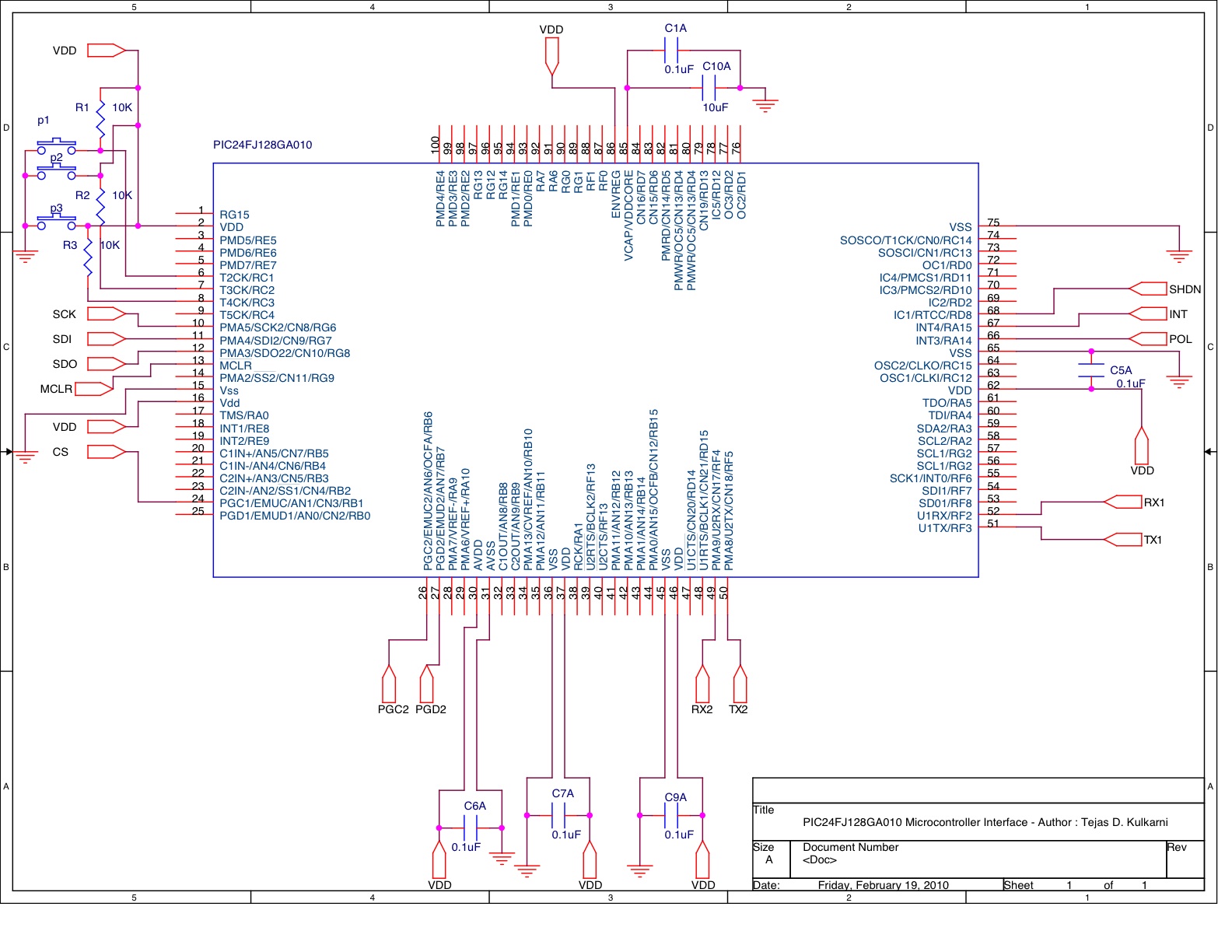
The PIC24F microcontroller is specified to run under a voltage range of 2V to 3.6V. The normal mode of operation is 3.3V. The low dropout regulator circuit provides the +3.3V for operating the microcontroller.In the proposed design, this device will interface with several digital peripherals – the battery gauge monitor, the Graphical LCD, Bluetooth module and the SD/MMC breakout. The design utilizes two UART modules, one SPI module, three digital pins for battery gauge monitoring and three digitals pins for pushbuttons. To program the microcontroller via Flash memory, a complete pinout is provided along with the necessary circuitry as per the microcontroller datasheet. I provided 4 pinouts for the flash programming - MCLR, PGD2, PGC2 and other power ground connection as specified in the datasheet for the microcontroller


The DX160 Graphical LCD used in the circuit takes a 5V supply voltage and can accept commands via a standard RS-232 or a TTL signal pins. The LCD can be connected directly to the PC RS-232 transmitter pin for easy debugging. The TTL signal pin cannot be directly interfaced with the PIC24F Transmitter pin (U1Tx). The PIC24F transmitter (UART) pin operates within the range of 0V to 3.3V. I found a Intersil CD40109BMS Low-to-High Voltage shifter to translate the 3.3V on the transmit(Tx) pin of PIC24F to 5V for the LCD's receiver (Rx) pin. It is important to note that the LCD does not have a transmit (Tx) pin due to the absence of any acknowledgement support from the LCD module. The LT1129-5 regulator provides the essential power to drive the Bluetooth module. The Bluetooth module is interfaced via the UART interface with the PIC24F microcontroller as shown in my schematics.
A SanDisk SD Card, operating at 3.3V, will be interfaced with PIC24F via the SPI peripheral interface. Since SD Cards are not tolerant to 5V, a LT1129-3.3 dropout regulator is used to provide a constant supply voltage of 3.3V for its operation.
February 19, 2010 (12 hours):
A consecutive all nighter in the lab - I worked on interfacing the SD Card with our design. I started interafacing it directly with the PIC24F. Earlier, me, Abhi and Ankur relied on using the 9S12 microcontorller. I soldered some pinouts on the Extension Card slot of PIC24F to interface it with our peripherals. I connected the SD Card according to the data I obtained from SanDisk SD card manual. I studied the format in which to read and write from the SD Card. I interfaced the card by placing it into a SD card Sparkfun card slot we purchased. Since the voltage levels of PIC24F and SD Card matched with each other, there was no use of any additional circuitry for voltage management.
Here is the circuit for the SD card interface with the microcontroller (as per the schematic I made the previous day).

To interface with the SD card, the SD has to be first initialized to operate in the SPI mode. I succesfully accomplished this since I got an acknowledgement from the card. I also tried reading 512 bytes of dats (default) from the SD card succesfully. However there were problems when reading. This is probably because I need to send CRC checksum as the last byte. The CRC calculation has the SD card Manufacturer's ID. I guess I am doing something wrong in computing the CRC. To verify, I hooked up Oscilloscope probes to DI and DO on the SD card slot to monitor the SPI communication. Look at the following illustrations :
1. Below, you can see the SPI CLK working the way it should be. Initially I had a lot of problems in initializing the SPI module for PIC24F since it was the first time I was writing code for it.


2. Here is the Inputs and Outputs obtained from the DO and DI from the SD Card breakout. The pictures showing one waveform represents the data going from Micro (DO) to SD Card (DI). The pictures illustrating two probes follow the following conventions - the signal at the top is from micro to SD card while the signal below is from the opposite. I verified to see if the signals were being sent the way they were supposed to be sent (and it was correct). Also note that the pictures are inverted horizontally. You can see in one of the pictures how the SD card responds after a few clock cycles once the PIC sends data commands of the output line (top signal)
Showing data from PIC to SD card (commands as per Sandisk datasheet):
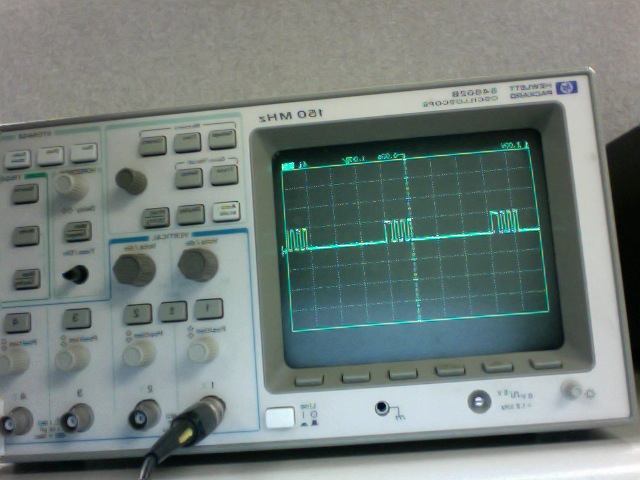

3. Showing data between PIC and SD card (commands and acknowledgements). You can see here that the SD is responding SUCCESFULLY -


February 21, 2010 (6 hours):
Studied the PADS tutorial and worked on the PCB routing and schematic. Also worked on revamping the image processing algorithm for the blob detection.
WEEK 06 SUMMARY
Accomplishments: Trying to interface Bluetooth and G-LCD. Bluetooth working. I individually finished the PCB schematic. Identified problem for bluetooth with David. Interfaced SD Card - Initializations and reading works properly
Weekly Work Total: 34 hours
Project Work Total: 90 hours
Week 07
February 23, 2010 (2 hours):
Worked on changing the schematic to include the new voltage shifter to translate voltage levels between the microcontroller and peripherals. The Graphical LCD and bluetooth operates with a voltage range of 0-5V. The microcontroller operates at 3.3V. Thus we needed a low-to-high level translator. We decided on using a MAX233 voltage translator for this purpose.
February 25, 2010 (3 hours):
The Total internal reflection of the multi-touch table is not accurate enough for blob detection. I went to the store and purchased everything I needed to remake the silicone sheet. I followed the exact same procedure described in my previous post by applied 3 layers instead of 2 this time. THe blobs were more accurate than usual. The other thing remaining is to tape the silicone rubber on the top covering sheet.
WEEK 07 SUMMARY
Accomplishments: Worked on revamping the multi-touch hardware. Worked on redesigning parts of the schematic to include the voltage level shifter
Weekly Work Total: 5 hours
Project Work Total: 95 hours
Week 08
March 1, 2010 (4 hours):
I completed and compiled most the Design review presentation for tomorrow (March 1,2010)
WEEK 08 SUMMARY
Accomplishments: Worked on the design review presentation
Weekly Work Total: 4 hours
Project Work Total: 99 hours
Week 09
March 11, 2010 (8 hours):
I worked with Ankur and Abhi to complete the PCB for manufacturing. Initially, we finished the routing then procedded with copper pour. I later on realized that we had connected the Vss and Vdd connections on the microcontroller in the wrong position. Also, the Avss and Avdd connections were floating. I read the MPLAB documentation and discovered that those connections are needed in order to program the microcontroller in flash mode. I made the appropriate connections on the schematic as follows:

March 12, 2010 (12 hours):
We realized that the ground plane connections and other connecting in the routing stage were disturbed due to some unknown reasons. Also, there were quite a few noticable problems with the routing such the width of the annular rings, the trace width of power and ground rails and other detail aspect. Instead of working on the already disturbed and complicated PCB routing design, we decided to recreate the routing for our schematic. This process did not take as long as we expected. After we completed our PCB, we placed all the components on the 1X printout of the PCB to ensure that all the pins on the PCB match with the actual physical pins. After the part list checkoff, we sent the design for to 4pcb.com for checks and recieve two major violations. The violations included :
1. Insuppficient Spacing violations:

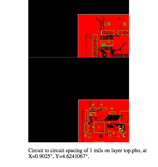

2. Annular ring violations
We were not exactly sure how to fix these errors.
March 13, 2010 (10 hours):
I met with Ankur to try to fix the violations from the check on the 4pcb.com website. Since it was a weekend, we could not get help from a course staff or the TA's. It took us a lot of hours before we could figure out the problem. The problem with insufficient spacing was with the issue of corerctly setting up the border of the PCB and the spacing between traces. We fixed the spacing problem by doing the copper pour first, followed by expanding the dimensions of the PCB. We fixed the annular ring violations by increasing the ratio (mills) between the inner and outer diameter. I also noticed a critical error in the DIR pin of the voltage translator and fixed it immediately. I also managed to port out a few extra pin-outs from the microcontroller. We submitted the design for dfm checking without any errors. The PCB submitted is as follows:
The final CAM output is as follows:
Cam-output 1
Cam-output 1


WEEK 09 SUMMARY
Accomplishments: Worked on finalizing the complete PCB and debugged errors in the PCB
Weekly Work Total: 30 hours
Project Work Total: 129 hours
Week 10
Spring break vacation - Did not spend any time on the project as I was out of town for a week.
WEEK 10 SUMMARY
Accomplishments: --
Weekly Work Total: 0 hours
Project Work Total: 129 hours
Week 11
March 27, 2010 (10 hours):
I worked on developing an API for communicating the Intel Atom board with our PCB via a bluetooth interface. I referred to the following link in order to develop the API :
http://developers.sun.com/mobility/midp/articles/bluetooth2/
I worked on interfacing the graphical lcd with the PIC24F micro. I also wrote APIs for drawing primitive shapes such as rectangle, square and lines. This is the circuit illustration of the graphical lcd (you can see basic primitives being drawn on the LCD).


March 28, 2010 (12 hours):
I spent quite a lot of time designing the GUI for the multi-touch table interface. I was trying to get the TUIO protocol to work (but without luck). For some reason, the TUIO protocol does not listen on port 3333 to detect the blobs from NUI CCV. I also played a lot with using Java2D, AWT and Java Swing.
WEEK 11 SUMMARY
Accomplishments: TUIO protocol implementation for blob detection. G-LCD works fine. Bluetooth API for Intel Atom
Weekly Work Total: 22 hours
Project Work Total: 151 hours
Week 12
April 1, 2010 (4 hours):
Worked with Abhisheyk on Patent liability analysis
April 3, 2010 (8 hours):
I worked with Abhi on developing the circuit for the Bttery charger IC. After a few minor problems, we succesfully tested the IC charger circuit on the bread board. We also hooked up a 3.7V li-ion battery from my phone to see if the voltage outputted by the charger was correct and it worked as per the expectation.
Below is the circuit for the IC charger without the battery. It should output around 8.6 V and it did. The output voltage is shown in the adjacent figure


This is the circuit with a 3.7V Li-ion battery. The output voltage is shown in the adjacent figure.


April 3, 2010 (9 hours):
Tested the IC charger circuit on the actual PCB. Soldered the IC on the PCB. The output voltage is shown in the adjacent figure
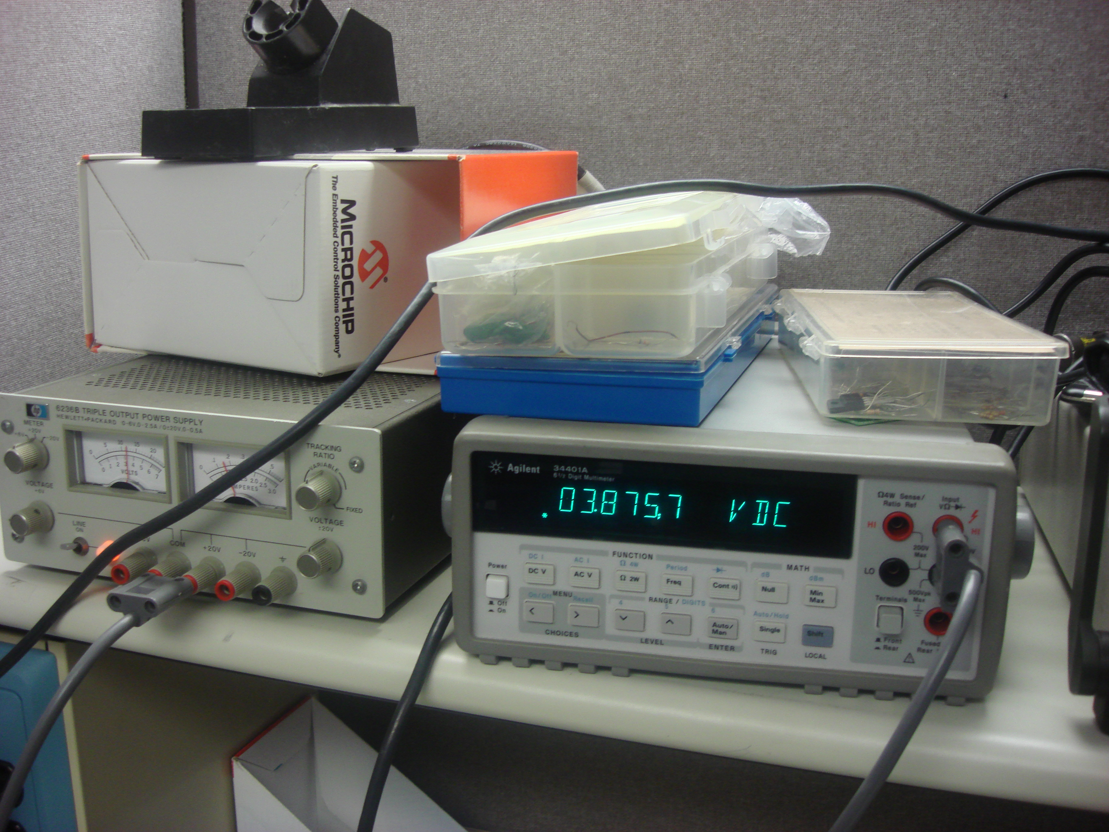

This is the circuit with a 3.7V Li-ion battery. The output voltage is shown in the adjacent figure.


WEEK 12 SUMMARY
Accomplishments: IC Charger circuit fully tested on the PCB
Weekly Work Total: 21 hours
Project Work Total: 172 hours
Week 13
April 8, 2010 (13 hours):
Worked with Abhisheyk on soldering the microcontroller to the board. We faced a lot of problems to program the PIC24FJ128GA010 in-circuit. The first problem was soldering the PIC24F microcontroller on our PCB. I had a lot of problems getting the extra solder off the chip due to slaggy soldering. Once the chip was soldered, we made other connections (voltage regulators) and the debugging header circuit to test the microcontroller. For hours, we could not get MPLAB 2 kit to talk with our microcontroller. After talking to Team 9, we verified our debugging schematic with theirs. We realized that there was an extra capacitor (0.1uF) at the MCLR pin.After hours of debugging, we inserted the capacitor at the MCLR pin and everything started working. It seems like the MPLAB 2 Microchip datasheet is wrong as the capacitor makes the reset stable. The datasheet explicitly says that the capacitor will destroy the microcontroller circuit and disable any debugging. I guess Microchip is wrong and we decided to term the capacitor as the "Magical Capacitor".
PIC24FJ microcontroller along with other debugging circuit and regulators soldered on the PCB

Backside of the PCB

Voltage regulators (3.3V and 5V output)

The entire test circuit connected to MPLAB 2 kit
PIC24FJ microcontroller along with other debugging circuit and regulators soldered on the PCB

The probable mistake in the Microchip datasheet
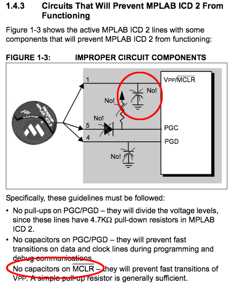
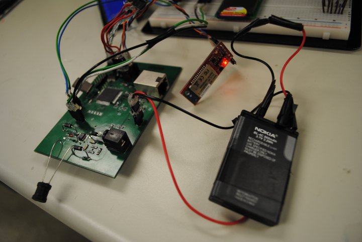
April 9, 2010 (12 hours):Worked with Himanshu on the PCB and interfacing the peripherals with the microcontroller. After discussing the debugging circuit with Himanshu, we tested in variety of conditions and saw that our microcontroller does not eexecute the program when the debugging header is removed from the jack. It seems like Microchip was RIGHT and we were WRONG! After carefully reading the datasheeet and experimenting for hours on fixing this problem, we made a modified circuit as per the guidance of a forum on the Microchip website. Now the "Magical capacitor" is removed and it works completely fine. With the presence of the capacitor, we observed unexpected and unstable mode that the micro goes in while programming. Now it works everytime we try to program it from the MPLAB software.
We also worked on soldering the voltage shifter and other peripheral circuitry with some fly wiring.
April 10, 2010 (12 hours):The voltage regulator circuit was not working the correctly. This resulted in failure to consistently program the PIC24F from the MPLAB kit. I was initially unsure why this was happeneing. After reading the datasheet, I found out that the voltage regulators need a Vdd+2V threshold to function. In our case, we were feeding the 8.4V to 5V and 5V to 3.3V. The problem was with feeding 5V to 3.3V. I read the MPLAB user manual and discovered that there the MPLAB kit can sense the voltage at the target. We knew that but then I found out that the MPLAB 2 GUI actually shows the Vdd at target in the power settings. I observed that the value marked was 2.5V. I instantly knew that the problem was with the regulators and me and Himanshu decided to change the conections for the regulator. I also worked with Abhisheyk on getting the Bluetooth and LCD to work together. He had figured out the way to change the clock from 8Mhz to 16Mhz. In the meantime, I was constructing the circuit to convert TTL to RS-232 in case we decide to use RS232 for GLCD. The main problem with the GLCD was that the factory settings are set when the TTL pin is connected to GND. In our case, our LCD would obviously be set to factory mode at the time of power up. The factory baud rate was 56k. In our case, we were struglling to get the PIC24F to get this rate without error. Abhisheyk figured out a way to set the PLL and get the baud rate to 56k. As described above, I constructed the TTL to RS232 pin as a backup plan since the LCD also has a RS232 connection. We managed to get the LCD and Bluetooth to work together. We also soldered the rest of the power components on the PCB. I observed that the multi-touch table does not smoothly recognize finger touches - I need to fix that asap.
WEEK 13 SUMMARY
Accomplishments:Microcontroller and almost all peripherals except the battery gauge soldered and tested
Weekly Work Total: 37 hours
Project Work Total: 209 hours
Week 14
April 13, 2010 (14 hours):
I started working on getting the TUIO protocol to work. I rewrote the entire code to pass on the blob co-ordinates to the Java Application. Initially the code was written in Processing because I thought that Processing would give us an edge to make a better GUI. I had to change my mind because there is minimal support for getting the Bluetooth API to work with Processing. We would pretty much have to port it with the IDE. It took me some time to write the TUIO handlers in Java. I spent a few hours to get the gestures to work with my Java Code. I also worked a bit on the code to initiate the multi-user "Experience". What the code does is it takes in a bundle of unidentified co-ordinates and groups them according to some heuristics for pattern recognition (gestures). As of today, I have made the code to detect the following gestures fool-proof:
1. Pinch and expand (scale)
2. Rotate two fingers close to each other for Rotation
3. Drag a finger to move objects
I have also started on working the main Graphical User Interface environment for the IDine Application. The illustration for the gesture recognition algorithm is as follows:

April 14, 2010 (14 hours):
I had been working for a long time on constructing simple apps for the main application program. Initially (like 2 months ago), I had proposed the idea of multiple apps that could be implemented to enhance the dining applications. As of today, I have completed the one of the few applications remaining in our project. I also wanted to make the interface very intuitive and with sophisticated graphics. As I have lots of experience in Computer Graphics, I started writing the main cover application in OpenGL to enhance graphics. The first app I made a few days back was completed today. The idea of the iDine system is similar to that of an iPhone - Multiple apps arranged in an intuitive fashion for easy access. Currently the iDine Java program consists of a framework I constructed which is scalable to any number of apps. Here are a few apps before taking a look at a snapshot of the entire application:
1. iDine Startup - A 3D animation displaying the Team name with user interactions
2. iDine Paint - An application I have been working on for a few weeks which is similar to MS Paint but just using finger blobs. It is fully custom built in Java using OpenGL
3. iDine Menu - The menu application with user interactivity (drag, select, rotate, scale)
4. iDine Dining area - I wanted to construct an app which will show some good looking graphics while the users eat food on the table (preferably interactive or touch sensitive)
5. Chef's special - An area with displaying "today's special items" with user comments and possibly small video clips
A snapshot of the entire system

April 17, 2010 (12 hours):
The SD Card is working properly now. I discovered a few problems with the SD Card. I fixed the MPLAB 2 project which dealt with the functionalities with the SD Card. After modifying the FAT16 library for our hardware setup and PIC24FJ128GA010, I discovered that we had to have a pull-up resistor on the SD Card hardware interface along with the decoupling capacitors. After further rewiring the circuit and testing for CLK and SDAT pins, I got the SD card to respond with the microcontroller. Currently, the SD Card can read and write files/directories on the itself.
WEEK 14 SUMMARY
Accomplishments: Multi-touch gestures and GUI development almost done. SD Card working fine with the micrcontroller 28 hours
Weekly Work Total: 40 hours
Project Work Total: 249 hours
Week 15
April 18, 2010 (12 hours):
Today, the final GUI with 4 applications were developed. The table was also brought to the lab and the entire setup was redone. I had also obtained the projector from Chuck the earlier day. We made the entire setup and tried to see if the table responded to the blobs. We observed that the blob detection was rough and was not sensitive. I applied another layer of Silicone and Xylol to make it make it extra sensitive. I also worked with the entire team on getting the Battery charger and integerating the cellphone batteries into our system. Currently, we are testing to see if the battery gauge correctly senses the battery life.
April 23, 2010 (14 hours):
Met with Abhisheyk and Ankur primarily to integrate all the components in the system using the new connectors we built earlier this morning. We also got all our PSSC checked off from Malek. Though we had installed all the components for the battery charger, there were some issues with the battery charger circuit when we installed all the components together. David has rightly pointed out the circuit to power the peripherals using the wall-wart when it is powered using an adapter. The circuit consisted of a diode between the power rail to peripherals and the battery to avoid any reverse currents. Initially, the circuit did not function as expected but everything started to work as soon as we discovered (after hours of debugging) that we needed a schottkey diode instead of a regular diode. Another problem was that the IC charger charged the battery at a very slow rate. We disassembled the spare Nokia phones and connected probes on the battery charger to observe the waveform outputted for charging the proprietary batteries. The wave outputted was some sort of a custom triangle wave with repeated pattern. We later on found from Linear technologies that the custom waveform is just to charger the proprietary batteries efficiently and we should be able to charge our batteries without any problem. The circuit in its full glory is as follows -


April 24, 2010 (13 hours):
Today, I applied another layer of silicone and Xylol to increase the touch sensitivity. Since this process takes about 6 hours, it is not possible to apply the ideal number of layers at one shot. As of now, we have four layer, which is 2 short from the recommended number of layers. I also ported rest of the gesture detection and camera processing units to make it compatible with the Atom board. Porting the basic GUI took me quite a few hours as the OpenGL libraries in the Atom board do not support reverse frame-buffering. I spent all day trying to display the basic layout of the menu bar along with gesture detection framework.
This is all we use for making the precious silicone layer -

April 25, 2010 (14 hours):
I spent some more time trying to write a keyboard as a means for writing feedback or comments about food items. Each keyboard can register one finger touch. Users can instantiate multiple keyboard in the same interface and close them at will. There is a button to send user feedback when the comment to be typed has fully been entered. I also spent quite some time on integrating the bluetooth driver with my multi-touch framework in Java. I researched upon the java.comm libraries and wrote some code to read and write raw bits between COM ports on the Atom board. Now, the Atom can successfully communicate with the PCB via the bluetooth module within the rest of the framework (Java).
WEEK 15 SUMMARY
Accomplishments: All five PSSC checked off. Multi-touch GUI ported to Atom board. Succesfully wrote and tested COM read/writes from Java to PCB
Weekly Work Total: 53 hours
Project Work Total: 314 hours
Week 16
April 27, 2010 (12 hours):
We worked as a team on programming the EMD device. The SD card interface was completed and the Java program was partially over which tries to open a COM port to connect to the Bluetooth device. Currently, there are issues with the bluetooth program since the connection is refused everytime the Java app tries to connect to the bluetooth device. I also wrote a parser to read bytes from the EMD to the Atom board. This parsed input will then be fed to the GUI to dynamically generate the menu items.
April 28, 2010 (14 hours):
We made the video for the presentation for tomorrow which took a lot of time. Here is the link for the video:
http://www.youtube.com/watch?v=YOVnTQDh7vY
I also developed three java programs to read in from the Serial input (COM3). There are problems with the connection since the Javaterm.java program crashes if not restarted everytime at connection. I also helped Himanshu and Ankur on the packaging of iDine.
April 29, 2010 (14 hours):
Since there was a problem with JavaTerm.java, we decided to write a C# program to open the COM ports and send the data to the Java program via a server-client application. Since the C# application was stable, we ended up writing the applications in that and opening a socket to talk to the iDine GUI program. We also encountered problems with the battery monitoring IC. The chip had unfortunately fried out due to unknown reason. Upon investigation, we found out that there might have been a short circuit in one of the refulators. We did see that the connectors were unconnected so we made new connectors and replaced the battery charger. So everything is working perfectly well including the battery monitor IC.
April 30, 2010 (14 hours):
Me and Abhisheyk finished witht interfacing the EMD to the iDine GUI via the C# bluetooth interface. The C# application is connected with the main Java application via port 19999 on localhost. We also revamped the video for today's presentation for the ECE 270 class.
http://www.youtube.com/watch?v=YOVnTQDh7vY
May 1, 2010 (5 hours):
Functionally tested the Java and finalized the C# server code. Currently, the C# server accepts bytes from COM3 on the Atom board. Here, COM3 represents the USB port where the bluetooth module is plugged in. The intermediate version of the server-client configuration can be changed via this simple GUI -
The point to rememer is that port 666 is reserved (on the Intel Atom board) once the iDine software starts running.

May 2, 2010 (5 hours):
Met with Ankur and finished the 477 Final report along with the poster. Apart from this, we also did a test run of the entire system at once.
WEEK 16 SUMMARY
Accomplishments: Prepared the video demonstrating the functionalities of the tabletop. Replaced the battery monitor and identified the cause of its failure (Voltage level difference). Interfaced the C# application with the main Java app for bluetooth communication. Finished the final report, poster and preparation for final check-off
Weekly Work Total: 64 hours
Project Work Total: 378 hours