Josh Smith's Lab Notebook
Week 01
January 12, 2010 (0.5 hour):
Met with team to briefly discuss project ideas and possible design implemenation.
January 13, 2010 (3 hours):
Met with team to further discuss project idea and complete the Team Building and Project Idea assignment. Discussion included applications, possible design schemes and possible design concerns. Wrote the prelimary draft of the assignment document with feedback from group. Mike Goldfarb to proofread.
January 15, 2010 (1 hour):
Met with Mike to set up lab notebook. Also, discussed possible DSP chips to be used in project. Currently considering both a SHARC and Blackfin from Analog Devices.
WEEK 01 SUMMARY
Accomplishments: Solidified project idea. Completed and submitted Project Idea assignment.
Weekly Work Total: 4.5 hours
Project Work Total: 4.5 hours
Week 02
January 19, 2010 (3 hours):
Met with team and Dr. Johnson to review preliminary project idea. Conclusion of meeting was to use an off-the-shelf transmission scheme and move forward with proposed DSP applications. Immediately following meeting with Dr. Johnson, met with Shao-Fu to catch up on project progress made over the long weekend. Convened with team again to discuss PSSC presentation and begin work on the Final Project Proposal. Wrote the preliminary draft of the Final Project Proposal.
January 20, 2010 (2 hours):
Finished the draft of the Final Project Proposal with entire team. Included deciding the project's final success criteria and creating a high level block diagram of the proposed audio system.
January 21, 2010 (2.5 hours):
Met with entire team to complete the Final Project Proposal. Ironed out the final PSSC's with help from TA's. Continued working with Shao-Fu to procure sample ADC's and DAC's from Texas Instruments ordering five DAC's and one ADC a piece. After placing the sample order, the estimated cost of the prototype was reevaluated using online suppliers. Concluded that the original estimate was approximately correct for the latest version of the design scheme.
January 23, 2010 (1 hour):
Met briefly with team to investigate the delay produced by running a signal through an FFT algorithm similar to what is planned in the design. Take away from meeting was a need to refresh C-programming skills and signal processing theory, namely the FFT algorithm.
WEEK 02 SUMMARY
Accomplishments: PSSC and project proposal finalized. Began procuring components for design.
Weekly Work Total: 8.5 hours
Project Work Total: 13 hours
Week 03
January 24, 2010 (3 hours):
Spent time refreshing skills needed for the design project in the form of C-programming and signal processing theory.
January 26, 2010 (2 hours):
Met with team to discuss FFT algorithm and windowing scheme. Team then reviewed feedback on the Final Project Proposal. The course staff determined the final proposed PSSC of an ability to switch between a wireless and wired input was trivial. Team tentatively decided to change final PSSC to an ability to control the volume digitally from the transmitter half of the design. Plan to confer with Dr. Johnson to ensure new PSSC is sufficient.
January 27, 2010 (3 hours):
First, team met with Dr. Johnson briefly to discuss proposed PSSC of digital volume control at the transmitter. Added difficulty of wirelessly controlling the system volume seems to be sufficient. Updated PSSC assignment to be sent to course staff for reevaluation. Next, met with the entire team. Supported Steve in effort to find an antenna meeting design requirements and constraints. The transmitting antenna will nominally have a 2.4GHz base frequency, 3 dB gain, have a relatively small package size, and low power consumption as the transmitter will be battery operated. Also, team discussed transmission scheme and bit error considerations with Malek.
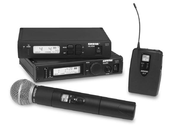
Later, began research for the Packaging Design Assignment. Was able to find wireless microphone systems similar to what is desired in the Digital Sound Projection (DSP) design. The Shure SLX Professional Wireless System is a close match to the current envisioned design scheme.
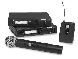
The system includes a transmitter box or wireless mic with antenna and user control features. A receiver box with LED display offers information on connectivity, selected frequency band, and battery life. The DSP design will encompass additional digital signal processing features requiring a more robust user interface in the form of LCD and push buttons. Will research sound boards to get an idea of how to combine the receiver and digital sound board pair.
January 28, 2010 (0.5 hour):
Met with team briefly. Called TI to order op amps but had no response. Will wait for response tomorrow or start searching TI's distributors (Arrow, Newark, etc.).
January 30, 2010 (4.5 hours):
Met with team to work on separate parts of project. First, researched possible components for use in the DSP design using Newark. Was able to identify and order both PDIP and SOIC TI op amps, a battery bay with 6" leads for the transmitter power source, and a 6V AC/DC wall wart power supply for the receiver base. All ordered parts fit current constraints of the system. The team also began researching LCD screens viable for use in the DSP user interface.
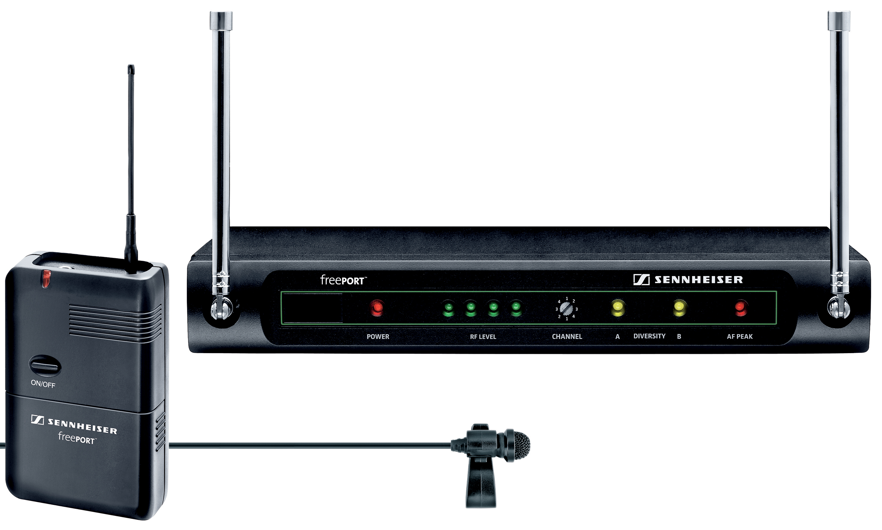
Also, continued work on the Packaging Assignment. Was able to find a second wireless microphone system similar in packaging design of DSP in the form of the Sennheiser freePORT Presentation Set.
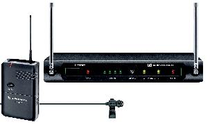
The set comprises of transmitter box and receiver base. The transmitter fits the small size constraint, ergonomically shaped for placement on a user's belt, and is battery powered. The receiver also fits the EMI shielding constraints needed for DSP although it is smaller in size and lacks the more robust user interface planned for DSP. Drafted Sections 1 and 2 of the Packaging Assignment.
WEEK 03 SUMMARY
Accomplishments: Began drafting Packaging Assignment. Continued parts procurement and research.
Weekly Work Total: 13 hours
Project Work Total: 26 hours
Week 04
February 1, 2010 (1 hours):
Met with Steve and Mike to discuss the some of the system constraints for the Constraints Assignment. More specifically, gave Mike the data found in researching similar package designs for his constraint analysis. Also, discussed a new possibility for the input scheme on the transmitter.
February 3, 2010 (3 hours):
Continued work on the Packaging Assignment. Researched IEEE reference notation and proofread first few sections of the document. Later, met with team and discussed packaging design possibilities.
For the transmitter, preliminary design will be small and light weight, a metal clip on the rear to allow user to attach to belt, and have a battery bay. There was some disagreement on the placement of the antenna; however, the preliminary design will have the transmitting antenna on the left side of the unit. Placing on the left side of unit is the best ergonomic choice as the antenna will not be an obstruction for right handed people and a minor obstruction for left handed people. Antenna placement on the left side of package will also minimize the package envelope.
Lastly, spoke with Malek to see what past groups have done to fabricate the packaging for their designs. Seems most designs have simply used a project box and DSP design will likely as well.
February 4, 2010 (3 hours):
Met with Steve and Shao-Fu and went to Lafayette Electronic Supply in hopes of purchasing components for the project. Were not able to find the desired inductors; however, were able to purchase a phone jack and power to PCB connector for prototyping. Upon returning, began work on the CAD drawing of the packaging scheme. Took a quick tutorial of the program suite and was able to draft a design for the receiving base. Will discuss with team and make improvements and changes where necessary.
February 5, 2010 (1.5 hours):
Continued work on Packaging Assignment. Polished errors on receiver CAD drawing and continued to make progress on the document.
February 6, 2010 (4.5 hours):
Drafted CAD drawing of transmitter package. Kept the package small and designed for user comfort and ease of use as transmitter will be worn on user's belt. Minimized the package envelope, placed LEDs and input jack on top of unit for easy access from above, and placed UI push-buttons on side for easy access on while worn.
Met with team to get feedback on initial packaging design. Will search for project boxes that fit DSP's size restraints and EMI shielding (aluminum box sealing gaps with copper tape) if possible. Also, completed the PADS layout, logic, and basic routing tutorials with some input from Steve. Worked through a few layout examples and completed the component decal for the TI headphone amplifier.
WEEK 04 SUMMARY
Accomplishments: Team completed Design Constraints assignment. Completed CAD draft of packaging design.
Weekly Work Total: 13 hours
Project Work Total: 39 hours
Week 05
February 8, 2010 (6 hours):
Researched project boxes and was able to find a reasonably sized ABS molded project boxes for both the receiver (8"x6"x3") and transmitter (3"x2"x1") at Radioshack. Also, continued to learn how to use the AutoCAD program. Created 3D models of the transmitter and receiver project boxes from Radioshack. Will search for aluminum project boxes for the receiver package to increase EMI shielding and reduce noise introduced from outside.
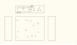
Later, met with Shao and Mike and worked on laying out the PCB footprint. Was able to finish a preliminary PCB footprint for the receiver board by considering all major components, passive components (namely 40 through hole capacitors), and separating the digital and analog portions of the circuit for EMI shielding considerations.
February 9, 2010 (8 hours):
Continued searching for aluminum packages for the receiving base. Located a reasonably sized aluminum project box at Parts Express in the shape of the Hammond 1590E Aluminum Diecast Case. This case meets all preliminary EMI shielding requirements the team has presently imposed for the receiver.
Next, met with Shao and Steve. Discussed packaging possibilities and settled on the Hammond 1590E Aluminum Diecast Case for the receiver and the Radioshack 3x2x1" ABS Project Enclosure for the transmitter. Now, with solid packaging dimensions, drew both the receiver package and transmitter package using AutoCAD 2009.
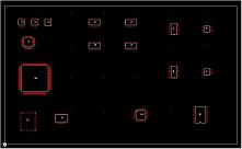
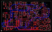
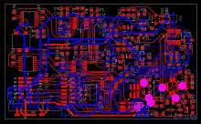
After completing the CAD packaging drawings, went back to lab to complete PADS layout of preliminary transmitter PCB. Using the size constraints from the transmitter package, chose a PCB blank of 2.8 x 1.8". Please refer to both the receiver and transmitter PCB footprints, respectively, below noting the receiver PCB size is 7.0 x 4.2".
PADS Receiver Layout
Transmitter PADS Layout
Lastly, put together the powerpoint slides for the Packaging PSCC to be given tomorrow. Also tweaked PAD layouts and CAD drawings for presentation slides.
February 10, 2010 (8 hours):
First, reviewed Powerpoint slides and made a few changes prior to presentation. Presented DSP's Packaging PSSC to the class. Dr. Johnson suggested using a rack mount and having the UI on the front face of the system. This suggestion will be seriously considered as it is the usual mounting scheme in the industry.
Next, continued work on the Packaging Assignment. Inserted all appendices into the report, namely the CAD drawings and PAD layouts of both the receiver and transmitter. Also, calculated the weights of both the RadioShack ABS package and Hammond Aluminum package by calculating the volume of each and multiplying by each material's density. The transmitter weight should be approximately 3 ounces and the receiver should weigh 2 pounds or less. After completing all appendices, proofread the document to ensure no mistakes are submitted with the final draft. Will confer with team tomorrow to get a final consensus on the document.
February 11, 2010 (1.5 hours):
Continued revisions on Packaging Assignment. Got feedback from both Mike and Steve, made final changes to document, and submitted final draft for grading.
February 12, 2010 (0.5 hours):
Ordered additional parts from Avnet and TI.
WEEK 05 SUMMARY
Accomplishments: Presented Packaging Specifications and Design PSCC. Completed CAD drawings of system package and completed PADS layout of initial PCB footprint. Also, completed Packaging Specifications and Design Homework.
Weekly Work Total: 24 hours
Project Work Total: 63 hours
Week 06
February 15, 2010 (3 hours):
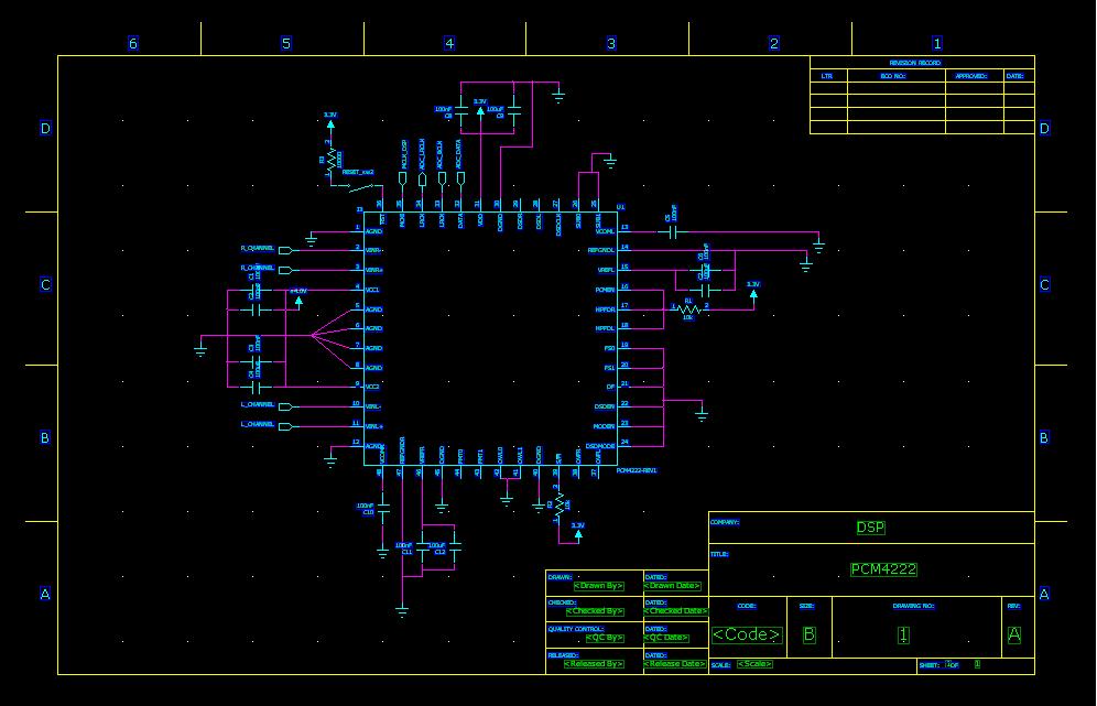
Met with team. Began laying out schematics in PADS Logic for preliminary schematics due on Friday. Began learning how to use PADS Logic more proficiently in the process of creating new schematics. Was able to lay out preliminary schematics for the transmitter PCM4222. Continued creating schematics with Steve as the day progressed.
February 17, 2010 (2 hours):
Met with team. Spent time tracking down TI parts (OPA4134 in particular) that seem to be out of stock at all TI distributors. Spoke with representatives from Newark, Arrow and Avnet to try to locate parts or find the shortest lead time available. Was able to find the shortest lead time at Avnet. Parts are due on March 12th meaning the shipment will come in over spring break. Also, contacted TI directly to see if there was any explicit reason behind the parts shortage and try to gauge when more parts will be manufactured. Was told there has been a much higher demand for their audio IC's than they had forecasted and they are doing their best to catch up with the market. Was also able to order additional sample parts during call with TI rep. Procured additional TL780-05's, DRV134's, and an additional PCM4222 ADC.
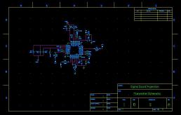
February 18, 2010 (4.5 hours):
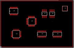
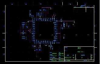
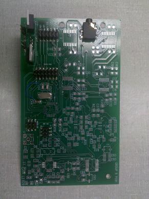
Met with team. Worked on revising and creating new schematics for the DSP design. Updated the DRV135 and the ADSP21262 schematics with Steve. Was able to start simulating parts that are not within the PADS Logic library, particularly regarding headers that do not exist. Was able to create a 26 pin header for the Sharc. Also, created schematics for the TPA6120A2 and the PCM4222 receiver layout. Please refer to pictures below, TPA6120 and PCM4222 receiver layouts respectively.
TPA6120A2 Schematic

PCM4222 Receiver Schematic
Also, determined what oscillators were to be used in design with team. Researched available parts on DigiKey and found relatively cheap crystals that met our design requirements.
February 19, 2010 (2 hours):
Met with team. Received parts from TI and Avnet (OPA2134, DRV134, TL780-05, and PCM4222). Supported Shao in prototyping the power regulating circuit. Had issues with noise created at the TL780. The average voltage level was correct but there noise was at an unacceptable peak-to-peak range, about 1V. After debugging, the correct configuration was found and was able to create a constant voltage with acceptable noise, about 50mV peak-to-peak.
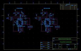
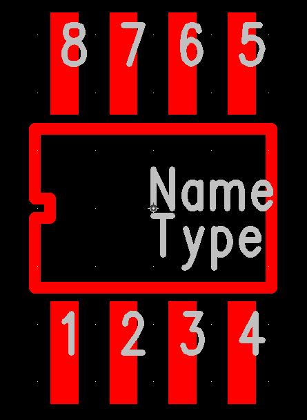
February 20, 2010 (3 hours):
Met with team. Went through the PADS Custom Footprint Tutorial on the ECE477 website. Using new knowledge, made custom footprints and corresponding logic layout for the TL780-05, LM317, and LM337 with support from Steve. Refer to picture noting all three components utilize the same packaging (and footprint).
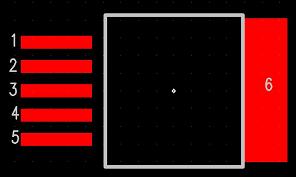
TL780-05, LM317, and LM337 Footprint

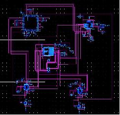
After creating custom footprints, created the preliminary logic circuit for the transmitter PCB with Steve. The preliminary layout was completed and then successfully exported to PADS Layout to ensure there were no major errors with the design. Refer to picture below.
Transmitter Preliminary Logic Circuit
WEEK 06 SUMMARY
Accomplishments: Completed preliminary schematics for a majority of the IC's and the transmitter module. Team completed and submitted Homework 5.
Weekly Work Total: 14.5 hours
Project Work Total: 77.5 hours
Week 07
February 22, 2010 (4 hours):
Met with team. Did research on parts and pricing for the OPA1611 and OPA54X series. Given requirements of the system, settled on OPA548 for the power circuit as it has an ouput current limit of 3A where the next version down had only 500mA which would be cutting it close if it even is enough current for the receiver. Researched pricing on all sites available and ordered parts from Mouser.
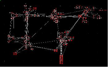
Next, began laying out the transmitter schematic for routing in PADS Layout with Steve. We isolated each chip and moved all passives close to their respective chip. Noted all mistakes found during process on layout. Will continue work tomorrow.
Rough Transmitter Layout
February 23, 2010 (4.5 hours):
Met with team. Worked with Steve on updating the schematic for the transmitter. Need to find an efficient way to route connections to the voltage sources of +3.3V, +5V, and -5V. With some help from David, was able to insert headers connecting the circuit to each voltage source. Also, learned how to update a layout with changes made in a linked PADS Logic file. Will be very useful as the logic circuit is updated to suit current project needs.
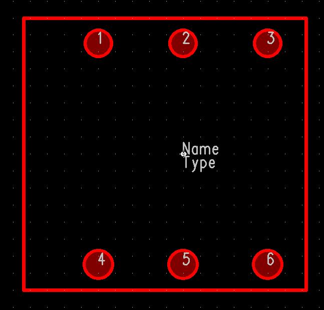
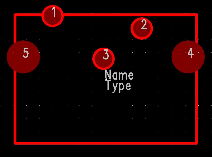
Also created a number of footprints for our circuit to accomodate new parts to be used on the PCB. Created custom footprints for the antenna connector and a variety of Nichicon electrolytic capacitors. Refer to pictures.
Antenna Connector Footprint

Nichicon Capacitor Footprint

February 24, 2010 (5 hours):
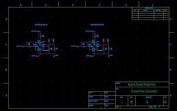
Met with entire team. Ordered additional TI parts needed for design (OPA1611, UCC384-5, PGA2505, REG104-5, REG104-33, DRV134, and PCM4222).
Contiued creating custom footprints and logic for components to be used in the design. Footprints and logic created today include the voltage regulators: UCC384-5, NJM7815A, NJM7915A, REG104-5, REG104-33, and the FAN1112.
UCC384-5
REG104 Series
FAN1112

February 25, 2010 (6 hours):
Met with entire team. Continued creating decals and logic chips for the PCB design in PADS. New decals and logic created include: AT25FS010, microphone input connector, and speaker RCA connector.
AT25FS010

Microphone Input Connector
RCA Output Connector
Also, created a schematic for the OPA1632 to be used in the receiver schematic. Began working on the preliminary receiver schematic through adding each major circuit and beginning to add connections between individual circuits.
WEEK 07 SUMMARY
Accomplishments: Completed decals for PADS layout. Continued to make progress on transmitter and receiver PCB's.
Weekly Work Total: 19.5 hours
Project Work Total: 97 hours
Week 08
February 28, 2010 (2 hours):
Met with entire team. Shortly worked on a new version of the transmitter layout as the original attempt left room for improvement. Made little progress before making the final decals, presumably, for the design. New decals included capacitors (Nichicon KZ 330uF, Panasonic ECQP1H272 and Panasonic ECQP1H222) and the power connector for the receiver circuit board.
Nichicon KZ Capacitor Decal

Panasonic ECQP Capacitor Decals

Power Connector Decal

March 1, 2010 (3.5 hours):
Met with entire team. Received large order of samples from TI including PGA2505, PCM4222, and power regulators.
Supported Steve in beginning to layout the receiver board. Once a computer opened up, I began working on the layout of the transmitter circuit board. Started by separating each individual circuit and becoming more knowledgable on the circuit designs in order to create the most compact PC board. Will start laying out each individual circuit and hopefully routing tomorrow.
March 2, 2010 (7 hours):
Met with entire team. Continued working on transmitter layout. Was able to isolate each major section of the circuit board and place components more efficiently to minimize routing and layout area as we have a limited amount of space for the transmitter. Also, was able to fix problems in the logic circuit found through prototyping, mainly in the addition of the OPA1632 buffer circuit between the PGA2505 microphone preamp and the PCM4202 ADC. Also fixed an issue with the PGA2505 logic circuit. Pin 22 was incorrectly connected and was changed to the correct connection of analog ground. Lastly, began putting together the powerpoint slides for the Midterm Design Review as a team.
Transmitter Layout Draft
March 3, 2010 (7 hours):
Met with entire team. Needed to complete routing for the Design Review presentation to be given tomorrow. In order to complete this, began routing the transmitter layout starting with the power circuitry. Was able to complete a portion of the power routing before using autoroute to complete the circuit as there was little time and the packaging design still needed to be updated. Issues to address from autorouting: at very least, must route the power and ground circuitry manually, must manually route the two channels separately, and must route the nRF transceiver circuit manually. Autoroute made some interesting mistakes but the three issues highlighted should address a majority of the problems.
Transmitter March 3
Upon completing the autoroute and analyzing the results, moved to the MSEE lab to update the packaging design to accomodate for the current PCB sizes of 6x10" and 3x5" for the receiver and transmitter respectively. Was able to find an aluminum die cast package of the correct size for the receiver in the form of the Hammond 1550J. For the transmitter, found a plastic package from Action Electronics of a size 5 1/4 x 3 1/4 x 1 9/16" to accomodate the larger PCB size. Note, both packages meet the original packaging constraints with the only difference being size.
March 4, 2010 (5 hours):
Met with entire team early to put finishing touches on the Midterm Design Review presentation powerpoint and work out kinks in the presentation. From there, the group presented our Midterm Design Review. David gave some good advice for the transmitter PCB in the form of spacing the surface mount components to avoid soldering issues and a problem with the oscillator/microcontroller layout. Began implementing design suggestions from David and starting routing the the right channel of the transmitter input circuit following the presentation.
March 5, 2010 (6.5 hours):
Met with entire team. Worked on routing the transmitter PCB. Was able to complete routing for the right channel components and the right channel portion of the ADC (PCM4202). Had to make a few changes in the general layout to accomodate routes that I had not previously anticipated. Two major shifts include the orientation of the PCM4202 circuit and the nRF24z1 orientation. There may be some potential routing issues with the nRF and microcontroller; however, am routing to accomodate in order to minimize difficulties with these chips. Also, need to learn about ground connections and ground plane considerations for the PCB. Plan on speaking with Chuck when he returns.
Transmitter PCB March 5
March 6, 2010 (6 hours):
Met with entire team. Continued work on the transmitter PCB routing. Began by resizing the PCB to 5x3" as the board was mistakenly made too large. The original layout did not fit on the new board shape. To accomodate the new size, the microcontroller and transceiver circuits had to be manipulated and moved to different positions on the board. After moving the circuits onto the new board, continued the routing process. Completed routing of the PCM4202 ADC, the nRF24z1 transceiver, and began routing the microcontroller. Need to find an efficient way to route the two large headers connected to the microcontroller.
Transmitter PCB March 6
WEEK 08 SUMMARY
Accomplishments: Completed Midterm Design Review. Transmitter PCB routing nearly completed.
Weekly Work Total: 37 hours
Project Work Total: 134 hours
Week 09
March 7, 2010 (3.5 hours):
Met with Steve and Mike. Continued work on the transmitter PCB. Changes and additions today include: added a pull down resistor to the nRF circuit, completed routing from the microcontroller to headers, nRF transceiver, and PGA2505 pre-amps, and rearranged the component silkscreens to assure the correct components are placed in their given location. Also, caught a few mistakes in the power circuitry in the design schematics. Updated and reflected changes into the PCB routing.
Transmitter March 7
Also, researched online parts catalogs for a single pole, single throw push button to be used for the transmitter user volume control. Was able to find a SPST push button rated for 12V and 0.3A on Digikey satisfying all of the design constraints.
March 8, 2010 (5 hours):
Met with entire team. Routed both analog and digital ground traces for the transmitter circuit board. Connected the two separate grounds at the power supply and sized traces accordingly. Need to verify the design before creating the final product and gerber files. Also, need to add team label, mounting holes and thermal pad connecting vias underneath the two OPA1632's as the chip has heat dissipation issues.
Transmitter PCB March 8
March 9, 2010 (4 hours):
Met with Steve in the morning to talk with Chuck about copper pours and ground planes in PADS. Was able to determine that the only area a ground plane is needed is under the nRF transceiver and a copper pour for thermal dissipation under the OPA1632 buffers.
Later, added the physical ground plane under the nRF transceiver. Began verifying the design using the built in PADS design verifying tool. Error instances were all acute angles as a result of awkward manual connecting points. Took the time to correct each acid trap with the exception of the acid traps between the ground plane and "X-connections" under the nRF. Will ask Chuck how to address this problem, assuming it is a problem that needs to be fixed. Also, reviewed the analog sections of the circuit with Shao-Fu to ensure there were no routing or logic mistakes. No glaring issues were found in the design so the team will be moving forward accordingly.
Transmitter PCB March 9
March 10, 2010 (5 hours):
Met with entire team in the morning to give the team's progress report to the course staff. Presented our problems with both my transmitter and Steve's receiver designs. Given Chuck's advice, the acid traps created between the X-connection and ground plane under the transceiver are non-issues as the traces are thick enough that the effect of the acid trap will be trivial. The team received no negative feedback as we are on schedule to complete the PCB designs by Friday and have all circuit board parts on hand.
Later, met with the team to continue work on PCB design. Worked with Mike to review the digital parts of the circuit. All connections and circuits were correct. Will be adding "Pin 1" indicators on the silk screen for each IC to ensure all components are soldered onto the board in the correct orientation the first time. Also, added silkscreens to clarify what each header is. Lastly, went through the CAM process to create Gerber files for the transmitter and submitted to freeDFM to ensure there are no "show-stoppers" in the design.
Transmitter PCB March 10
March 11, 2010 (3 hours):
Met with entire team. Received the freeDFM report on the transmitter PCB. There were 37 possible "show-stoppers" on the board in the form of "possible solder-mask clearance issues". Spoke with Chuck to see what action to take for the possible issue. Chuck said the solder-mask clearance is a non-issue so no action will be taken to correct the warnings.
Next, updated the PADS logic schematics for the transmitter for the Proof of Parts presentation to the TA's. The circuit boards were CAM'ed one to one and each unique component was placed on the print outs. David checked our design and components and had no major issues.
Lastly, added finishing touches to the transmitter PCB. Changes included adding mounting holes, adding final silkscreens previously missed, and ensuring each silkscreen was not interfering with another.
Transmitter PCB March 11

WEEK 09 SUMMARY
Accomplishments: Verified correctness, completed and submitted the PCB design for the transmitter. Work included completing the PADS routing and lay out of the transmitter circuit and checking work with team to ensure no design flaws.
Weekly Work Total: 20.5 hours
Project Work Total: 154.5 hours
Week 11
March 23, 2010 (3 hours):
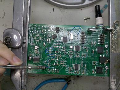
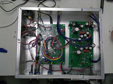
Met with entire team. Received fabricated PCB's from Chuck. Began testing circuit using the PADS schematic as a reference. Was able to check the 3.3V, 5V and -5V power traces, the analog and digital ground traces, and the analog components of the left and right channels. Two mistakes on the circuit board were found in the process of verifying the board.
First, a ground trace connecting the digital ground to both PGA2505 pre-amps was missing. Simple fix is to jump the ground pins of C44 and C54 together. This will connect the currently floating ground to digital ground. The second issue is an entire trace connecting the SDO pin of the two PGAs to the microcontroller. Whether this was missed in a lapse of judgement or a PADS issue, the fix is to jump the three pins together (both PGAs pin 7 to micro pin 16). All other connections were correct along the two channels, power, and ground. For tomorrow, will check the digital portions of circuit and ADC.
March 24, 2010 (2.5 hours):
Met with entire team. Continued working on verifying all connections on the transmitter circuit board. Checked all traces from the nRF transceiver, ATmega microcontroller, and the 4202 ADC. All connections functioned correctly.
Also, after convening with Mike, the PGA2505 routing issue was found to be a non-issue. The trace was removed from the design as the trace added trivial functionality to the system. The only remaining issue is to fix the floating ground by fly wiring the two capacitor pads mentioned in yesterday's lab entry.
March 25, 2010 (1.5 hours):
Met with entire team. Shadowed Shao in order to learn soldering basics. Learned how to solder and inspect a small SOIC chip onto a circuit board.
After leaving the lab, continued learning how to solder through reviewing online resources and how to clips. Plan to practice in lab upon returning from Iowa.
WEEK 11 SUMMARY
Accomplishments: Tested connectivity of the transmitter circuit board and found solutions to all connectivity errors found during the process.
Weekly Work Total: 7 hours
Project Work Total: 161.5 hours
Week 12
March 29, 2010 (1 hour):
Met with Shao briefly. Shao briefed me on events I missed during my on site interview in Cedar Rapids, Iowa. Continued to catch up on the power issues found through reading Mike and Shao's lab notebooks. Plan to begin work on the Ethical and Environmental Impact Analysis document the next few days as I will be away from the lab for another interview process.
March 30, 2010 (5.5 hours):
Met with entire team. Learned how to physically solder using a practice board. After getting some feedback on soldering ability, began soldering the power regulators onto the transmitter circuit board.
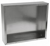
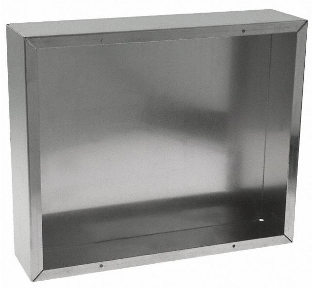
Also, researched new packaging design for the receiver package as the final design was different than the PCB size the package was designed for. Using Digikey, Steve and I were able to find an aluminum sheet metal chassis that met the size requirements of the design at 12x10x3" and material requirement for EMI shielding considerations. The package also leaves some space available in case there are any last minute design changes requiring more real estate.
Receiver Package
March 31, 2010 (3 hours):
Met with entire team. Continued work on soldering components onto the transmitter circuit board. Completed and tested the power supply of the transmitter. The three voltage regulators of 3.3V, 5V, and -5V all output the correct voltages to the respective traces on the board. After testing the power supply, soldered all headers onto the board. Lastly, began soldering the microcontroller circuit onto the board. Progress included the microcontroller 4MHz oscillator and all passives with the exception of the LED resistors. Will complete the microcontroller circuitry and continue work on the transmitter upon return from Halliburton on Saturday.
April 1, 2010 (2 hours):
Began working on the Ethical and Environmental Impact Analysis homework. Began brainstorming potential ethical and environmental issues inherent to the prototype. Also, wrote a brief outline pertaining to the most pertinent ethical and environmental issues with the design.
April 3, 2010 (4 hours):
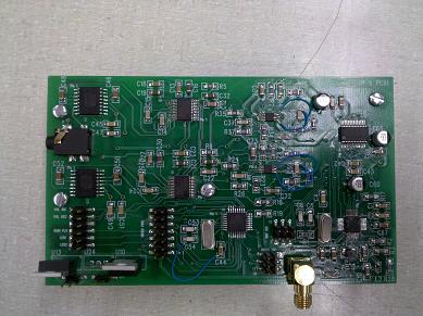
Met with entire team. Continued working on the transmitter circuit board after catching up on progress made while I was in Oklahoma. Steve was able to complete the DRV and PGA circuitry and found an issue with the microphone input footprint which will be resolved via fly wiring from the connector's position in the package. Progress made today included completing the PCM4202 circuitry.
Transmitter Circuit Board 4-3
Also, made a trip to pick up the project box for the transmitter and push buttons to be used on each unit and received the physical receiver package in the mail. The bottom section of the package was not included with the aluminum casing so the bottom sheet metal cover was ordered from Digikey.
WEEK 12 SUMMARY
Accomplishments: Began process of soldering components onto the transmitter circuit board. Circuits completed included power, DRV differential generator, PGA pre-amp, and PCM4202 ADC. Also, began work on the Ethical and Environmental Analysis document.
Weekly Work Total: 15.5 hours
Project Work Total: 177 hours
Week 13
April 5, 2010 (2.5 hours):
Received a call from Digikey informing that the receiver package cover that was ordered on Saturday was not in stock. Searched for the package cover, found it in stock at Mouser, and ordered. The cover should come in with ample time to complete the necessary machining for the package design.
Later, met with entire team. Continued work on soldering the transmitter circuit board. Shao and Steve soldered on the OPA1632's with the new fly wired configuration. I soldered the remaining discrete components into place to complete the OPA1632 circuitry. Plan on testing both the op-amp and ADC circuitry tomorrow.
Transmitter Circuit Board 4-5
April 6, 2010 (4.5 hours):
Met with entire team. Tested the OPA1632 circuit with Shao. After some miscommunication, the circuit was correctly investigated and found to be functioning as expected.
After testing the op-amp circuits, Shao soldered the nRF transceiver chip onto the board as my soldering skills are not quite good enough to handle a QFN package. After Shao verified the nRF was soldered correctly, I soldered the remaining components onto the transmitter circuit board. There are only two remaining components to solder, two LED resistors whose value have not been determined as a LED color has not been chosen.
Transmitter Circuit Board 4-6
Lastly, helped Shao with the RMS document. Proofread and gave suggestions regarding the document. Upon completing proofreading, began reading the article in relation to the Ethical and Environmental Analysis document.
WEEK 13 SUMMARY
Accomplishments: Completed soldering components onto transmitter circuit board. Verified transmitter functionality.
Weekly Work Total: 7 hours
Project Work Total: 184 hours
Week 14
April 11, 2010 (6 hours):
Began work on the Ethical and Environmental Analysis document. Was able to complete the introduction, ethical concerns section, and started the environmental analysis section using relavent sources such as the EPA and RoHS (Restriction of Hazardous Substances) websites.
April 12, 2010 (1 hour):
Continued work on the Ethical and Environmental Analysis document. Found additional resources to reinforce the solutions found for the environmental issues. Will hopefully complete both the document and presentation tomorrow.
Also, met briefly with team to catch up on work missed while taking care of a family emergency out of town. The transmitter and receiver are communicating successfully and with little added noise to the final signal. The majority of work for the project seems to be done!
April 13, 2010 (6.5 hours):
Met with entire team. Soldered LED's onto a header to be used on the transmitter circuit board. The LED's will indicate power and data link with the receiver.
Also, completed preliminary work on the Ethical and Environmental Analysis document. Will begin proofreading process and get feedback from the rest of the team.
April 14, 2010 (1 hour):
Presented the Ethical and Environmental Analysis regarding the Digital Sound Projection project. Received some good feedback regarding NiMH batteries and ethical concerns, especially regarding frequency sniffing. Will be changing and adding sections to the analysis document to ensure accuracy of information and that all major ethical and environmental concerns are covered in the analysis document.
Later, met with entire team to investigate why the system can only transmit successfully over a 2-3 meter range where a range closer to 30 meters was originally expected. Met with Professor Chappel to investigate this issue in the RF lab. The transmitter was investigated and found to be transmitting a power level more than sufficient for the range expected. Therefore, the issue must lie somewhere on the receiver matching network or the antenna itself. Investigation to be continued.
April 15, 2010 (5.5 hours):
Met with entire team. Continued work on the Ethical and Environmental Analysis document. After some research regarding feedback from the TCSP presentation, added relevant information regarding the project that was previously missed. Received help from Shao in proofreading the document and then submitted the final document to the ECE477 website.
Also, made a trip to Radioshack with Shao to find double pull, double throw switches for the transmitter power circuit. Were able to find a few options. Shao rigged the power switches into the transmitter packaging and the power switch functions correctly.
April 17, 2010 (4.5 hours):
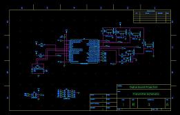
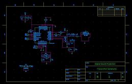
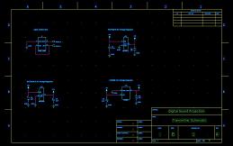
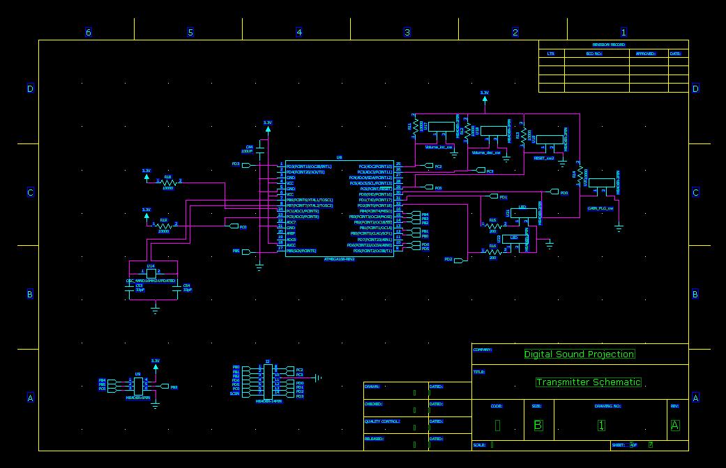
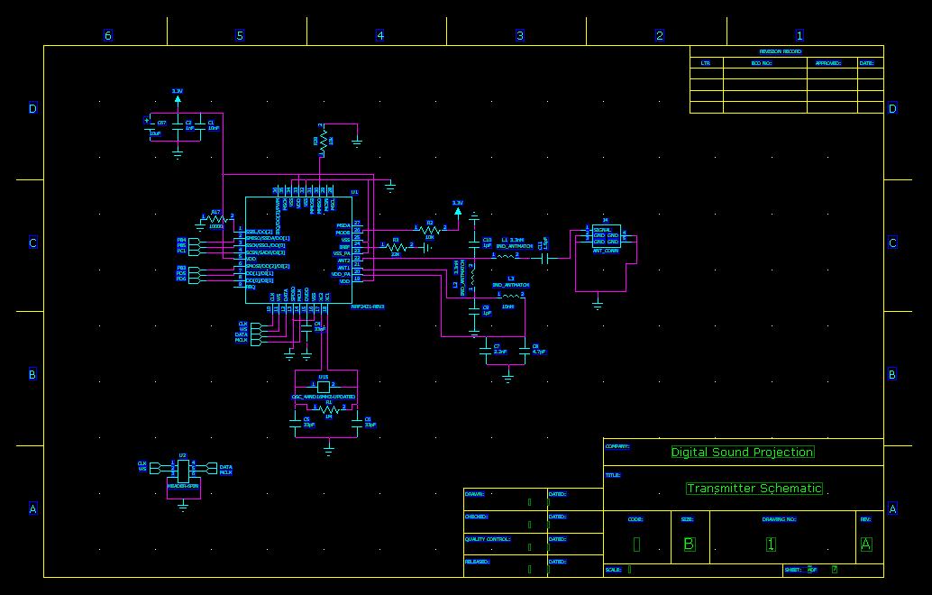
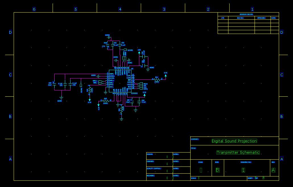
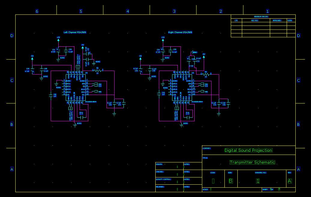
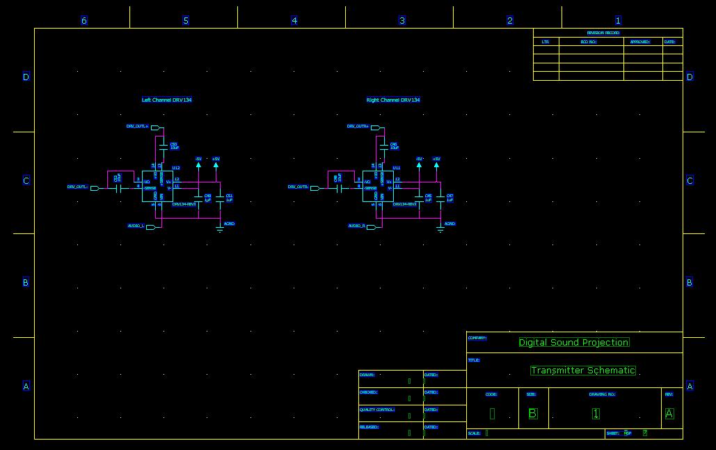
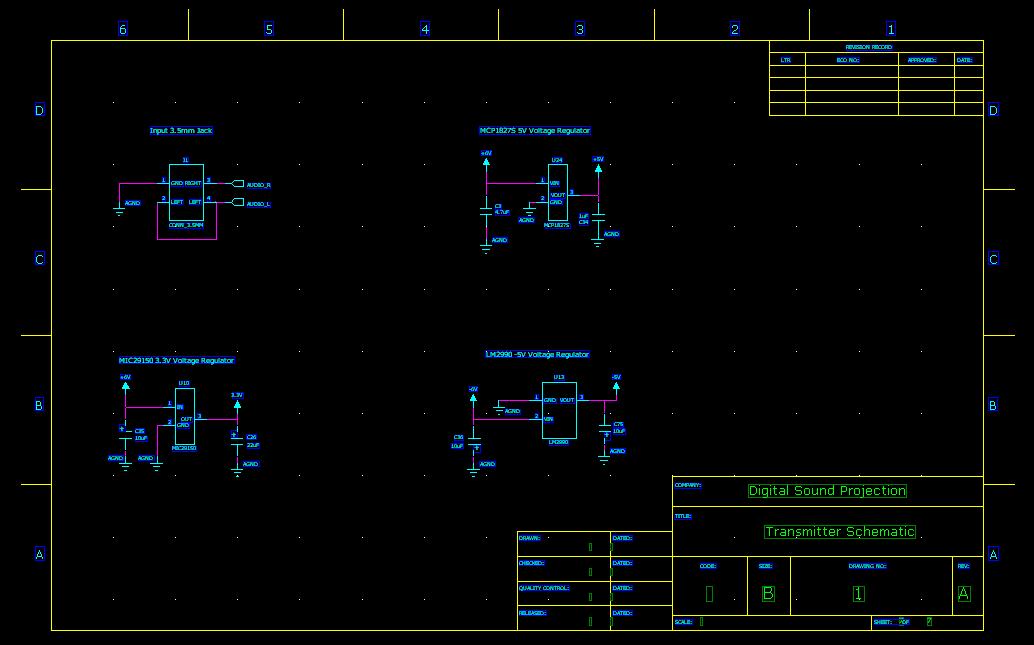
Met with Steve and Shao. Worked on bringing together a final version of the transmitter schematic. Separated individual circuits (ATmega168 microcontroller, PCM4202 ADC, nRF24Z1 transceiver, PGA2505 pre-amp, DRV134 differential generator, and power) and consolidated into one PADS file with multiple sheets. Refer to attached pictures for final schematics.
Transmitter Final Schematics
WEEK 14 SUMMARY
Accomplishments: Completed the Ethics and Environmental Analysis for the Digital Sound Projection design. Completed the Ethics and Environmental TCSP presentation in class. Finalized a version of the transmitter PADS schematics.
Weekly Work Total: 24.5 hours
Project Work Total: 201.5 hours
Week 15
April 20, 2010 (4 hours):
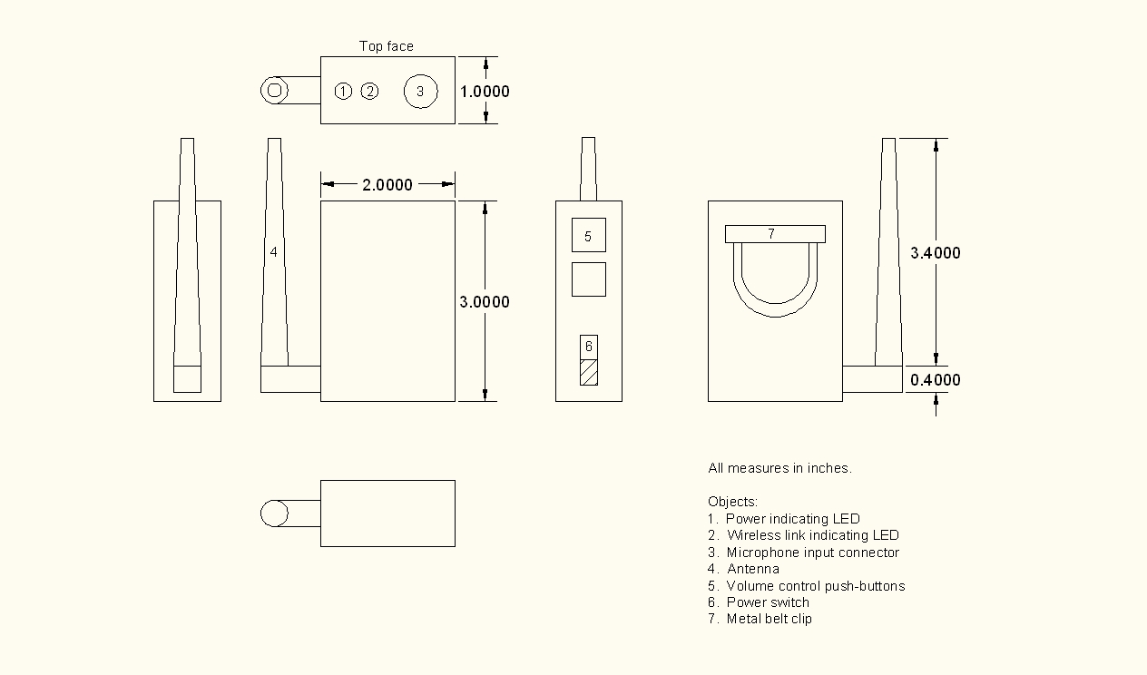
Met with entire team. Made a trip to Radioshack and Walmart to purchase new power switches for the transmitter, gorilla glue to secure the rotary encoder in place on the receiver, and to find a solution to labelling both packages.
Upon returning with the new parts, assisted Steve in writing the user manual. Took pictures to insert into the report and helped proofread as we went through the report.
April 22, 2010 (4 hours):
Met with entire team. Took more pictures for the user manual as Chuck provided a label maker and the packaging changed accordingly.
Later, began work on the final report. Pulled all of the graded materials from the ECE477 website and corrected subsequent formatting issues. Will be addressing all comments made by the course staff and updating the packaging drawings, updating the BOM, and pulling together the remaining work from the team.
April 23, 2010 (3 hours):
Met with entire team. Continued working on the Final Report. Pulled BOM's from the three circuit boards and other necessary figures to insert into the report with Steve's help.
April 24, 2010 (2 hours):
Continued work on the Final Report. Pulled together the final parts list for the transmitter. Need to finish the parts list for the analog and digital boards of the receiver unit.
WEEK 15 SUMMARY
Accomplishments: Began work on the Final Report document including updating original reports and figures. The team demonstrated DSP's PSSC's in lab.
Weekly Work Total: 13 hours
Project Work Total: 214.5 hours
Week 16
April 26, 2010 (4.5 hours):
Met with entire team. Continued work on the Final Report. Steve helped pull PDF's of copper and silkscreen layers of all three circuit boards to be inserted into Appendix D. Mike is still working on finalizing the schematics to be inserted in Appendix C. Shao-Fu to review the schematic narrative section to ensure up to date technical details. Progress on the report today included inserting PCB copper layers (missing inner layers of receiver digital circuit board), adding the final PSSC's, and making corrections from graded material currently available on the course website.
Also, Shao-Fu added insulated wiring connecting the analog circuit board to the new RCA connectors effectively completing the receiver packaging scheme.
April 27, 2010 (8 hours):
Met with entire team to complete the project completion briefing with the course staff. Take away from the meeting was to try and address the wireless range issue. The system currently has an effective range of about five meters and the staff would like a more robust range. There are two ways to address the issue with the receiver antenna matching network by either replacing components on the matching network empirically until the wireless range is improved or use an uni-directional antenna on the receiver to increase the antenna gain by two or three. To address this issue, Shao-Fu and I went to try and find an uni-directional antenna in Lafayette but had little luck. Shao-Fu to look online tonight.
Also, progress on the final report continues. I completed my section of the team contributions, completed the rough parts lists for both the transmitter and receiver units, and inserted the RMS section of the paper. Will meet with Steve and Mike tomorrow to get the remaining prices as they have the project receipts. Also, will hopefully be able to insert the remaining schematics, insert the packaging drawings, finalize the PSSC fulfillment, and complete the remaining sections.
April 28, 2010 (3.5 hours):
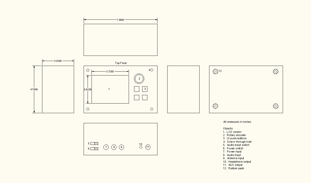
Met with entire team. Presented the functioning PSSC's in front of the class. After the demo, worked with Steve to finalize the parts list and review what else needed to be completed for the Final Report. Also, updated the transmitter packaging illustration as the design changed after the midterm design review.
April 29, 2010 (4 hours):
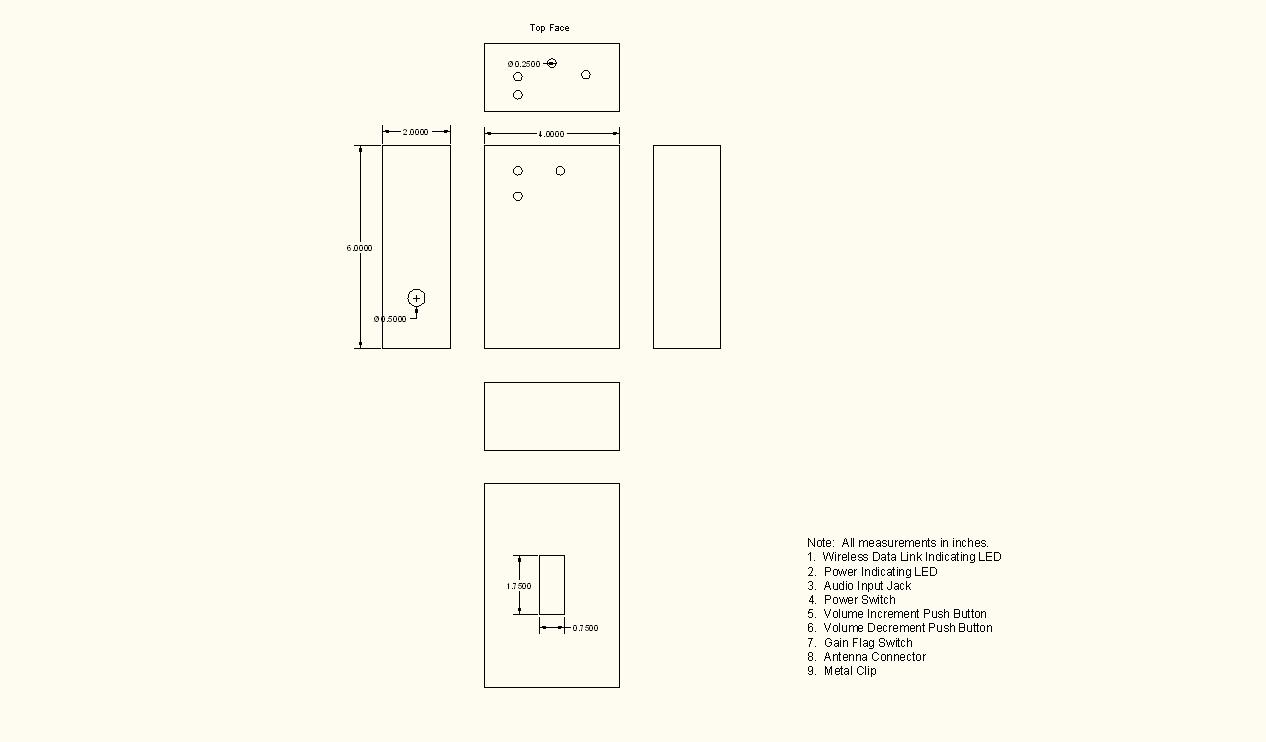
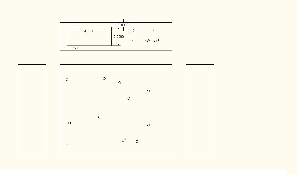
Met with entire team. Continued work on the Final Report. Completed the finalized receiver packaging illustration for the report.
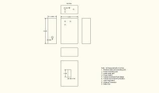
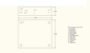
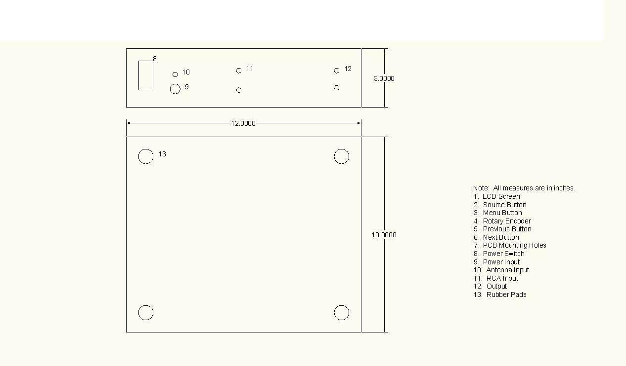
Receiver Package Top, Left, Front, and Right Face
Receiver Package Rear and Bottom Face
Also, updated the references section and ensured all hyperlinks were "hot". All that is left to finish is the abstract, the project overview, version 2 changes, and the summary; all of which should hopefully be done by tomorrow.
April 30, 2010 (6 hours):
Met with entire team. Continued work on the Final Report. Inserted the final schematics into Appendix C, inserted and proofread Shao's personal contributions section, went through and addressed remaining grader's comments, and wrote the project overview section. Only remaining action item is to update the block diagrams for Section 1 of the document.
Also, the team presented our project and PSSC demonstration to both the ECE270 and ECE362 classes.
May 1, 2010 (2 hours):
Met with entire team. Worked on the final presentation powerpoint and completing the final documents remaining. Submitted the senior report and user manuals after final proofreading. Steve reworked the final poster as the original file was corrupt. Only remaining action items are to practice the final presentation and complete the block diagrams to be inserted into the final report and poster. Will submit these two files upon completion.
WEEK 16 SUMMARY
Accomplishments: Completed majority of final documentation assignments. Gave bonus presentations to ECE270 and ECE362. Began preparing for the final presentation.
Weekly Work Total: 28 hours
Project Work Total: 236.5 hours


