January 13, 2009 (1 hour): Discussed project ideas
January 14, 2009 (1 hour): We wrote homework one
January 15, 2009 (2 hours): I looked for ways to control a large
number of leds and I looked at different reed switches and touch sensors for possibilities
for how to sense the chess pieces. Link to TI LED Drivers Atmel touch sensors
WEEK 01 SUMMARY Accomplishments: This week we finalized our project idea. I started
to look at details of led drivers and methods of sensing the chess
pieces. Weekly Work Total: 3 Project Work Total: 3
January 22, 2009 (2 hour): I emailed a representative from Atmel's
Qtouch division. He seemed interested in our project and is going to send us some sample
parts and an evaluation board.
I also looked a quite a few reed switch companies. The most promising looks like
Hamlin.
WEEK 02 SUMMARY Accomplishments: This week I found a lot more information on touch
sensors and got samples ordered. I also narrowed down our search for
reed switches. Weekly Work Total: 3 Project Work Total: 6
Week 03
January 25, 2009 (1 hour): I was looking for ways to read data from
all the inputs from the reed switches and I found this
website. It used and SPI I/O extender to look at a matrix of 64 switches. I'm not sure if
we will want to do this exact route, but the I/O extenders are very interesting.
More information on these is at Microchip's Website.
They have both SPI and I2C versions. There addresses can be set with external resistors and
eight can be used on the same bus.
January 25, 2009 (3 hours): We all met as a group to talk over the
project. We looked into reed switches and magnets and Matt is going to contact Hamlin
Sensors to see about getting some samples. We also looked at magnets for the chess pieces.
We found the ID of the base of the chess pieces were all just a bit larger than 1/2".
We found some rare earth ring magnets with OD of 1/2" and ID of 9/32". These should be
able to be mounted in the base of the chess pieces and still allow the light from the
LED to illuminate the piece. We found these at www.amazingmagnets.com and
www.magnet4less.com. Hussain is going contact www.amazingmagnets.com and ask about a sample.
January 26, 2009(1 hour): I looked over Atmel's offerings and found their
Parametric Product Table.
Looking over this I found the ATmega128
to be interesting. It has a lot of peripheral, all the standard things. It also has two UARTS
which could be useful if we want to have a RS232 port for debugging.
January 27, 2009(1 hour): I spent some time looking over LED drivers. I was able to find two that were the most
interesting. The TLC59116 and the
TLC5940 . The 59116 is most promising because it communicates
over I2C and has no other interface requirements other than being compliant to I2C. This would make the wiring between the main board
and the board with the leds and reed switches very simple. It doesn't, however, come in a through-hole package and it doesn't have
as many digital dimming steps (it's a 256 level pwm) as the TLC5940 (it has over 4000). The TLC5940 is spi and has more features, but
also has more interface requirements.
January 28, 2009(1 hour): I look for LEDs online from parts suppliers, but the most cost effective source seems to be ebay.
I was able to find some RGB LEDs and have a very wide viewing angle (around 140 degrees) that will probably work very well. They are called
"strawhat" leds and have a stubby lens on them that not only widens viewing angle, but also gives them a lower profile than standard through-hole
parts. Here is the website for the ebay seller.
Another big plus for these parts is the price. They are vastly cheaper than I can find through digikey et cetera. I ordered twenty to evaluate them.
January 29, 2009(1 hour): I was looking online at electronics projects and found the Cornell microcontroller class
webpage.
There I found a team that had done a similar project where they used reed switches on a chess board. The reed switches they used will not
work for our application (they were full reed sensor products that are too big for us). But there is some good information on talking to
the large switch matrix.
January 30, 2009(.5 hour): The LEDs and LED drivers came in today and I spent some time looking over them. The LED drivers
are smaller than I thought they would be. They have a .65mm pitch. I don't think we will have any problem with that, but they also have one pad
on the bottom. We should be able to work with them because this pad is just for heat dissipation and not an electrical connection. I looked and
found a SSOP to DIP adapter breakout board on Sparkfun
that will help us with protoptying the LED drivers.
January 31, 2009(2 hours): We met at a group to start working on homework 3 and to finalize some parts decisions.
We assigned different subsections to everyone. We also decided to go with the I2C LED driver since it was simpler to interface with.
WEEK 03 SUMMARY Accomplishments: This week I ordered and received some RGB leds and sample LED drivers to
test. I found I/O expanders and started to work on Homework 3. Weekly Work Total: 10.5 Project Work Total: 16.5
Week 04
February 2, 2009(1.5 hours): I met with Hussain and we worked on getting some simple blinky code
on the ATmega168 and I have. We were able to figure out that you use the avr/io.h library for the port pin names
and that you use util/delay.h for the delay functions. We are having some trouble getting the make file to work.
February 3, 2009(3 hours): We all met today and worked on Homework 3. We also finalized our
choice for Microcontroller. We decided to use the ATmega64. It has the same feature set at the ATmega128 that we looked
at before, but it has a little less flash. This chip has all the peripheral that we need, and enough pins to have enough
GPIO pins. Matt and I tested the leds and reed switches. The switches are not sensitive enough to be separated very
far from the magnets, we need to figure out how to get the reed switches closer to the bottom of the board, get stronger magnets,
or some combination of the both. Finally, I walked to Chuck and got a development board for the atmega128 and asked about some
smt to DIP adaptor boards.
February 4, 2009(1.5 hours): I met with Matt in the Lab and talked to Karl and Chuck about the Project.
We talked about how if the reed switches are mounted vertically (perpendicular to the circuit board) we get more sensitivity from
the magnet/reed switch, but it also makes the "bleed over" effect from a magnet from the next square less of an issue. Chuck also
found some smt to dip adapters, so I can solder our parts to them for prototyping. Chuck had the idea of just soldering a wire onto
one end of the reed switch and mounting it vertically like you would with a through-hole resistor. Finally, Karl thought that we
should just use the ATmega128 since it had double the flash as the ATmega64. Since it is a prototype we might as well use the bigger one.
February 5, 2009(3 hours): I finished up the assignment on design constraints. I also talked to John about his
ideas about how to calculate possible moves and check and check mate. Check and check mate are going to be much more difficult than
calculating the possible moves for a random piece. I also thought about the way to work the displaying software. I think that we
could use an 8 by 8 by 6 matrix. This would allow there to by six bytes for each chess square, two for each color. Each color
would have the current color byte, and the operation byte. A scanning function would look at the specific square and modify the current color
according to the operation byte.
February 6, 2009(2 hours): I met with Hussain and we got some simple blinking led software successfully programmed
onto the ATmega168 and we had. I also did some practice soldering and then attempted to solder up one of the smt to dip adaptor boards.
I got the pins slightly misaligned so I will need to desolder it and try again. I also called Atmel and requested some ATmega128 in QFP packages.
WEEK 04 SUMMARY Accomplishments: This week I finished up homework 3. I also ordered sample microcontrollers from Atmel.
I also worked with Hussain to get some code written and programmed to the ATmega168. Weekly Work Total: 11 Project Work Total: 27.5
Week 05
February 9, 2009(2 hours): I soldered the smt to dip adapter for the led driver chip and did a conductivity test to check that
nothing was shorted out. I have it to Hussain so he could start trying to talk to it over I2C. I also met with the team and we talked over the packing
choices for the packaging homework assignment.
February 10, 2009(1 hour): I soldered the smt to sip adapter for the touch sensor IC and checked it for conductivity. I also
read through the data sheet again for the part. I am pretty sure that we want to use it in slow mode with the sync pins of the two devices connected
together. This allows them they synchronize so that the scanning of one capacitive pad doesn't interfere with another pad. Also, based on the fact that
the "tuning" capacitors for the touch sensor pads are in the nF range and they stray capacitance of a breadboard is in the pF range, I think that we
will be able to breadboard the touch circuits without must problem.
February 11, 2009(1 hour): I met with mat and tried out the 1/2 OD x 1/4 ID x 1/8 magnets that came in the mail. They are probably
too strong because the pieces will want to snap together when they get very close. This would probably cause all the pieces on the board to bunch up
whenever the player moved. I looked on amazing magnets again and found some other ring magnets that we missed before. They are the same OD, but are thinner
and have a larger ID. These come in axially and diametrically magnetized verities, so I requested some samples of both so that we could try and see which are better.
February 12, 2009(5 hours): I was contacted by a representative from amazing magnets. He is going to send us some samples of each
of those magnets and they should be here mid way through next week. I also made pcb symbols for the ATmega128, TLC59116, QT240, and the RGB LED. I was
looking into the diodes to use to solve the "ghosting" issue with the switch matrix, and I found some common cathode dual diodes in a sot 23 package.
This would let us reduce the parts count and sot 23 is also a very easy package to solder. The part number is BAV74.
February 13, 2009(2 hours): I made the I/O expander and reed switch symbol. I also started working on the switch matrix schematic.
WEEK 05 SUMMARY Accomplishments: This week I got the smt to dip adapters soldered, worked on magnet selection, and made several schematic symbols. Weekly Work Total: 11 Project Work Total: 38.5
Week 06
February 16, 2009(4 hours): I worked on the schematic today. I reworked the switch matrix and worked on the LED array. I also helped
Matt get started on the main controller board.
February 17, 2009(5 hours): I worked on the schematic a lot more today. I finished up the switch and LED array. I fixed some issues with
the address registers on the I2C LED drivers. I helped Matt worked on the main controller board some more.
February 18, 2009(2 hours): I tracked down an LDO to use for the main power, part number ld29300xx18. I found a schematic
symbol for this part in the online database. I also found a schematic symbol for the small LDO for the touch sensors.
February 19, 2009(4 hours): I finished up the rest of the schematic and cleaned up some errors and inconsistencies.
February 20, 2009(2 hours): Matt and I started working on the PCB layout. We got some DRC errors on the schematic and worked through all of those.
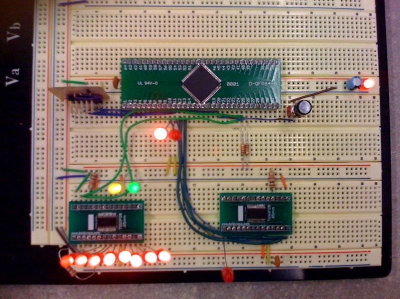
February 21, 2009(6 hours): We all met and worked on PCB layout and some "hello world" code for the microcontrollers.
I spent a lot of time making footprints that weren't in the library (most of them). I finally got everything linked with a footprint, and I
then got some error with the big LDO that I got off the part database that cause the process to crash. Layout Plus then was nice enough to
tell me that it wasn't going to save.
WEEK 06 SUMMARY Accomplishments: This week I worked on and finished the schematic and started working on the PCB. Weekly Work Total: 23 Project Work Total: 61.5
Week 07
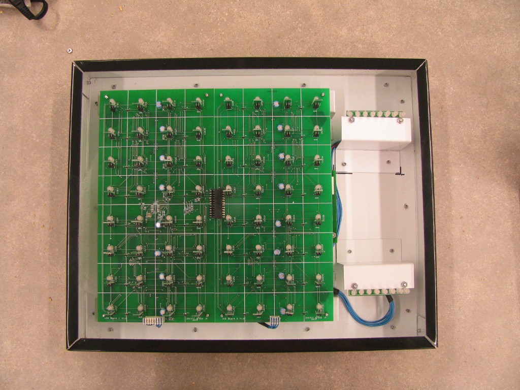
February 22, 2009(4.5 hours): We all met again and we decided to start working on the LED and switch matrix board. I made
a 5mm RGB LED footprint and started on the layout. I was able to get all the parts on the board and in their approximate location on the board.
I also helped the other guys out working on getting some simple SPI and I2C code working, which was successful.
February 23, 2009(4 hours): I got the LEDs and reed switches in their correct locations. I also got the switch matrix traces
placed on the board. Fortunately, the matrix is mostly on the top copper, with only a few small vias for the horizontal traces to jump over the
vertical traces.
February 24, 2009(5 hours): I worked on running power and ground traces and had a lot of trouble getting the rubber bands
to "re snap" to the large power rail that I ran along one side. As a result when I ran traces to the power rail they wouldn't terminate there
and would leave a rubber band connected to some other random pad. I also started the layout of the LED driver I2C and pwm traces. I tried to get
the I2C traces as unobstructed as possible, but they are still a little screwy.
February 24, 2009(3 hours): I realized that the way I had the LED drivers on the board was going to lead to a big mess with
lots of vias with the PWM lines. I figured out that if I placed all the LED drivers in a column up the center of the board they I could run the I2C
and SPI lines up the center, and all the LEDs on the left side of the chips would be connected to pads on the left side and all the LEDs on the right
would connect to pads on the right. This eliminates traces crossing over the center of the board and gets the PWM lines away from the data lines.
This will hopefully reduce noise on these.
February 25, 2009(3 hours): I worked on the new layout for the LED/switch board. I was able to run the traces up the middle
of the board and started figuring out the PWM traces.
February 26, 2009(5 hours): I finished the bottom half of the LED/switch board. There are still lots of vias in the PWM lines
but the I2C and SP1 lines are nice and clean. I am still having lots of problems with the Power and, to a lesser degree, the ground nets. There are
rubber bands that are snapping to other pads across the board, even though they are already connected to the net.
February 27, 2009(2 hours): I finished up the I/O expander traces. I also talked to chuck about the idea of using the layout
for the first LED/switch board. My idea is to make a copy of the schematic and layout and then make changes to the schematic to make it match the
schematic for the first board. Then I will make the necessary changes to the board. Doing thish should save a lot of time as compared to starting
from scratch for the second board.
WEEK 07 SUMMARY Accomplishments: This week I worked a lot more on layout. I was able to finish off the LED/switch board. Weekly Work Total: 26.5 Project Work Total: 88
Week 08
March 1, 2009(2 hours): The whole group met to talk about the design review. We talked about who would cover what topics.
I also helpd Matt with the main controller board. We were able to use the Atmel application note and get the crystal layed out and we also
just worked to clean up what was there.
March 2, 2009(5 hours): I finished up the LED/switch board. I helped Matt work on the on the main board some more. We also
got everthing ready for the design review.
March 3, 2009(3 hours): I worked with John on some SPI code. We cleaned up the code and started converting it over to a library
We also looked into what kind of data we needed to send to the I/O expander. We also figured out how to actually to a read when the micro is an SPI
master. Basically, the read and the write happen at the same time. So when data is shifting out of SPDR (SPI Data Register) on MOSI, it is also
shifting into SPDR from MISO. So in order to do a SPI master read only, we have to send 0x00.
March 4, 2009(1 hours): We got the breadboard adapter board for the mega128 in the main today and I soldered that part and made a
ISP header to breadboard adapter with some protoboard.
March 5, 2009(4 hours): I wired up the breadboard with the Atmega128 and the Led driver and I/O expander.
I also converted some of our old code over from the Atmega168 to the 128. Since AVR-GCC is so well done all I had to do was change the mcu tag in the make file to m128.
To get the I2C to work I had to disable the ATmega103 compadibility mode fuse bit. Since the 128 is compatible with the old ATmega103, it ships with TWI and some other
things disabled that were added to the 128. To change this you have to program the fuse bits of the ATmega128. I found a
website that has a fuse bit calculator and was
able to use it to figure out the new fuse settings. The command that I used to program the fuse bits in avrdude was:
avrdude -p m128 -c usbtiny -U lfuse:w:0xE1:m -U hfuse:w:0x99:m -U efuse:w:0xFF:m
WEEK 08 SUMMARY Accomplishments: This week I worked mostly on moving from the older ATmega168 to the newer ATmega128. The included both porting the code from one to the other and
setting up new hardware. Weekly Work Total: 15 Project Work Total: 103
Week 09
March 9, 2009(4 hours): I worked with Hussain on trying to take to the I/O expander over SPI. We are having come problem getting it to work. What we have found
is that there was an inconsistency in the documentation. It said that when set an output, a write to the GPIO register is the same as
a write to the output latches (OLAT), but we found that we couldn't get anything to work unless we wrote directly to OLAT. After we got this to work
It quit working. We were having problems getting anything consistent to happen. What I think what happened is that when I soldered the I/O expander to the
breadboard adapter I overheated the chip and damaged it. We have spares, but I found that there is a DIP version and I decided to order one.
March 10, 2009(3 hours): I met with Matt and helped him work on the main control board. we worked on remaking the oscillator circuit with a new ground pour. I also helped Matt fix some oddities in his
power traces. This was mostly just straightening them out or moving them to run in more logical places.
March 11, 2009(5 hours): I met with the group and we had the design review. I was mainly focused on the PCB layout. We didn't have too much to change, but the main thing was to add more bulk capacitors to the LED boards to
help prevent any fluctuations due to the PWM on the LEDs. Also, I experimented with using a gerber editing program to panelize the reed switch breakout boards. This wasn't looking too promising so I think
that we should just make them on their own board instead of trying to add them to the main controller board.
March 12, 2009(7 hours): Today I made the changes from the design review to out PCBs. I also worked with Hussain on laying out the reed switch breakout board. Since the circuit was so simple (just a reader and switch) we were actually
able to just layout all the parts and use the auto router to do the routing. I also made a complete copy of the schematic and layout of LED board 1. I think edited the schematic to make it the same as led board 2
and then made the necessary changes to the layout. This meant that I didn't have to start from scratch for LED board 2. This made the whole process much quicker.
March 13, 2009(4 hours): Today I worked on finishing up the PCBs and generating the files for submission. These were completed and submitted to Chuck. At last, PCB layout is done!
WEEK 09 SUMMARY Accomplishments: This week we had the design review. After the changes were made from this I mostly was focused on just getting the PCB layout done. Weekly Work Total: 23 Project Work Total: 126
Week 10
March 18, 2009(2 hours): I got an email from Chuck saying that boards 1 and 2 (the LED boards) were rejected because I used a via with a 12 mil hole and that the minimum hole size was 15 mil. I made the necessary changes to the padstack
and moved traces that now had a violation. I recreated the postprocess files, did another freedfm check and send the updated files to chuck.
March 19, 2009(1 hour): I got another email from Chuck saying that the main controller board had the same via hole size issue and I corrected it.
WEEK 10 SUMMARY Accomplishments: This week I fixed the problems with our PCBs that were keeping them from being manufactured. Weekly Work Total: 3 Project Work Total: 129
Week 11
March 23, 2009(3 hours): I worked with the new DIP I/O expander chip today. I was able to replace the chip that we had soldered to a breadboard adapter
with the DIP part and get it working. Also, with the old malfunctioning chip we wouldn't write to the GPIO registers and get
it to work correctly, now everything works as described in the I/O Expander data sheet. We can successfully read and write to the chip.
March 24, 2009(2 hours): Hussain and I worked on writing the interrupt service routing for the SPI. The way it is written, the whole scanning of the board
happens inside the ISR which keeps sending out the correct data until the board is scanned. The data is placed in a global matrix so that it will be able to be accessed by other
functions. To start the process a dummy send has to be initiated in the program (probably in a timer ISR) that starts the SPI ISR running and scanning the board.
March 25, 2009(6 hours): Today Matt and I picked up the reed switch breakout board PCB built all of the boards. We used the sheet metal shear in the EE
machine shop and then spent several hours soldering them all together. They are now all complete, and I have tested about half of them with the multimeter to ensure that we
weren't damaging the reed switched due to thermal shock during soldering.
March 26, 2009(1 hour): I met with Hussain and John and talked about the software homework.
WEEK 11 SUMMARY Accomplishments: This week I built the reed switch breakout boards and worked quite a bit on SPI software. Weekly Work Total: 12 Project Work Total: 141
Week 12
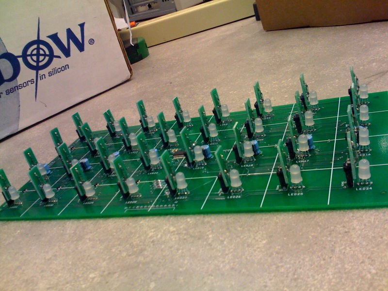
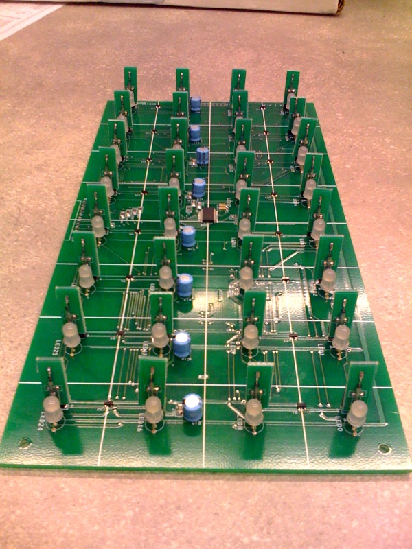
March 29, 2009(6 hour): We got the LED/reed switch PCBs back from Advanced Circuits and I soldered the first one together today. There was only one mechanical
issue with the boards. I found that when I placed the footprint for the female header to the reed switch breakout board I did not take into account the thickness of the breakout board.
As a result there was not enough clearance between the reed switch and the LED. I was able to make it work, however, by angling the LED slightly. This ended up working out because the
LEDs are diffused and they make a wide enough beam that it will still illuminate the square enough.
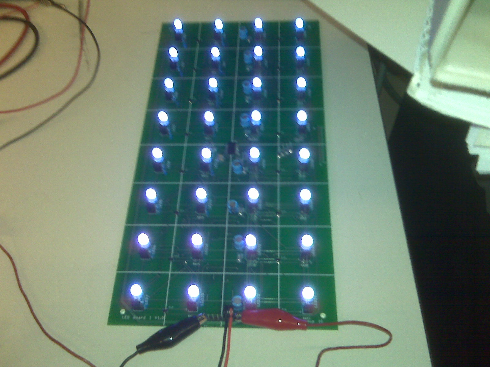
March 30, 2009(1 hour): Matt and I looked over the LED/reed switch PCB and I soldered yesterday. We didn't find anything obviously wrong with it (cold solder joints, bridges, etc)
and so we decided to hook it to our ATmega dev breadboard and test it out. We were able to successfully run the test code that turned all LEDs on. When we maxed out the brightness of all LEDs
it pulled about 2.5 Amps. In order to keep the current under 1A we had to lower the PWM register to 0x80. We should probably look into changing the Rext and the IREF register so that the
maximum current on each doide in the RGB LED is close to 16 - 20 mA. This would put the maximum brightness of the board closer to 1A.
March 31, 2009(4 hours):I soldered together the second LED/Reed switch board. It was also tested and all the I2C led drivers work.
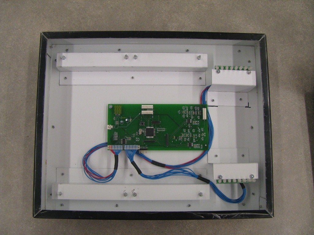
April 1, 2009(2 hours):I worked on the Microcontroller board. I built power supply and tested it by driving both LED boards with the power supply.
It gets pretty hot to the touch. I think this is still within the limits of the part but we may want to add a headsink to the part to help with this. I also soldered the
LED driver for the timer LEDs, the ATmega128, and some of the headers. I tested the ATmega128 by loading code onto it and everything looks good.
April 2, 2009(3 hours):I tested some more code on the ATmega128 on out microcontroller board by ensuring that the "blinky" code blinked port C.
I then tested I2C by hooking the main controller board to the LED/Reed boards. This code still ran as expected. Everything looks good on the microcontroller board so far.
April 3, 2009(3 hours):I tried to test out the SPI chip on the LED/Reed switch board. I ran the same code (the non interrupt driven code) that is
known to work on the DIP I/O Expander on the breadboard. The chip didn't respond. Matt and I used an oscilloscope to double check that the signals were getting to the chip correctly.
We also checked the schematic and the layout to ensure that everything was hooked up correctly. Everything we looked at was correct. We came to the conclusion that the I/O expander
was damaged during soldering. I spoke to Chuck and he is going to help me remove and solder the spare I/O expander. If this dosen't work the contingency plan is to green wire the DIP
I/O expander into the board.
WEEK 12 SUMMARY Accomplishments: This week I finished soldering the LED/Reed switch boards and did half of the main controller board. I was also able to ensure proper functionality of the LED drivers
and the main controller board power supply and microcontroller. Weekly Work Total: 19 Project Work Total: 160
Week 13
April 5, 2009(2 hours): Matt and I got interrupt drivert UART working. We used a circular buffer scheme very similar to what we used in ECE 362.
We got it all working and then found that because there is so much overhead in the printf function it is never able to put the second character in the buffer before
the first is sent out.
April 6, 2009(3 hours): I looked into how we should save the game state. I looked at flash, but it is very complicated and involved. Fortunatly, our
chip has EEPROM. It is a lot easier to deal with and there is already a library for using it in AVR libc. I would some good examples at AVR Freaks.
In the library there are six macros that let you read and write a byte, a word, or a block of memory. See the tutorial for more information.
April 7, 2009(4 hours): I met with Chuck to get the I/O expander replaced. After that we tried to run the original code on the DIP version on the breadboard. We were unable to get the code running. We're not sure why the chips are dying, but
we thing we might have some ESD damage. It seems like a long shot because we weren't really messing with it since we last ran code on it. Anyway, we decided to scrap the whole IO expander since we have had so many problems with it.
April 8, 2009(2 hours): I started looking a serial to parallel, and a parallel to serial shift register to use to replace the faulty I/O expander. I settled on using the 75HC595 serial to parallel, and the 74HC165 parallel to serial. The 595
has both internal and external latches. The data is clocked into the chip just like a normal shift register, but does not actually go onto the pins until a pulse on the latch pin. This will let the chip ignore the dummy send when we read data back from the parallel
to serial shift register. I bought both parts and started working with them on a breadboard.
April 9, 2009(4 hours): I worked with the shift registers and got them working with the ATmega168 and a small, 2x2 matrix of pushbuttons. The code is in SPI_library_new.
April 10, 2009(4 hours): I built the new shift register circuit on protoboard and ensured that it still worked with the small 2x2 matrix on the breadboard. I next wrote the function SPI_scanboard. To use this you jsut pass the address of a 1x8 array and the function
fills it with one bit for every swuare on the board. I chose to do it this way so that the data would be 8 byts, instead of the 64 bytes that would be necessary if I used one byte for each square. The problem with it is that it has the board in the wrong orientation. The bits from row three are in column three. To fix this I need to invert the matrix bitwise.
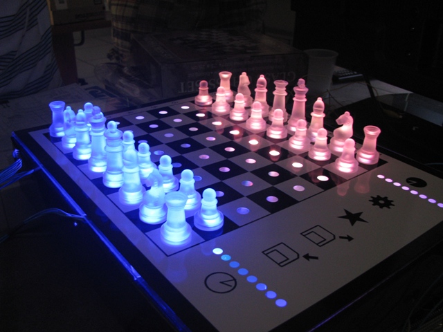
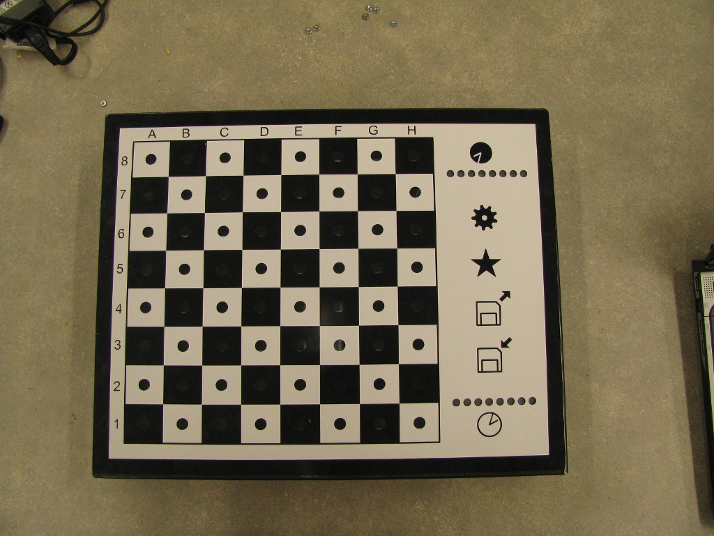
april 11, 2009(6 hours): I worked with my Dad to build the sheet metal box that we are using to hold our game. It is 12x15x2 and is made of gloss back aluminum with a clear acrylic plastic face for the chess board. We got the box built assembled.
WEEK 13 SUMMARY Accomplishments: This week I got issues with the I/O expander finally sorted out (be scrapping it) and got the box made for the board. Weekly Work Total: 25 Project Work Total: 185
Week 14
April 13, 2009(3 hours): Today I soldered the shift registers on the protoboard into the LED/Reed switch board. I tacken on wires onto the bottom of the right angle header and on to the female headers for the switches on columns 0 through 3.
After I had it soldered in I did some quick testing and so far everything looks good.
April 14, 2009(5 hours): I did some more testing on the shift registers after porting the code form the mega168 to the mega128. Took some time to get it ported over, but it is working now.
I also helped Matt design some of the vinyl that will go on top of the acrylic face to be the chess board surface. We got the basic grid of the board and some preliminary
layout work done for the touch inputs.
April 15, 2009(4 hours): I went with Matt to Auto Graphics in Lafayette and asked about the pricing on the vinyl. For two colors (black and white) of vinyl to be ready to apply (cut, weeded, and assembled in transfer paper) it will be aobut $50-$60.
We decided that this was reasonable and decided to go with this shop. I also worked on designing some icons for the touch sensors. I have a save and load icon, along with icons for the two clocks.
April 16, 2009(5 hours): I finished off the icons and asked my room mates and various other people to tell me what they ment. I found that everyone pretty much got save, load, settings, and the timers, but almost nobody got the new game icon. I changed
it to a star and it was understood a little better. I also got the SPI code wotking with the UART code and wrote a short program that reads the state of the board inputs and prints it out to the screen. This all worked out, except that the matrix of bits still needs to be
flipped to have the correct orientation.
April 17, 2009(3 hours): I worked on a function that would invert the matrix of bits. I tried to get it to work with a nice clean line of bitwise operations, but I wasn't working and it was too complicated to debug so I decided to go the easy route
and just use two nexted for loops with an if statement that built the new bit patterns for the inverted matrix. This code was tested and works perfectly. It is called SPI_fixboard and is in the SPI library file in SPI_library_new.
April 18, 2009(2 hours): I realised that there weren't any standoffs in the lab that were long enough to hold the LED/Reed switch boards high enough
(we need the boards about 1.25 inches from the bottom of the case). Matt and I looked for longer bolts at the hardware store, and I looked in a Granger catalog and still
couldn't fine anythign longer than 1 inch. Since I couldn't find anything I decided to make some 1 inch brackets to bound the PCBs on. In addition to being the right height
these should be much more stable than the bolts would have been alone. I also have some 2 inch brackets to hold up the LED timer PCBs
WEEK 14 SUMMARY Accomplishments: This week I finished off the SPI drivers and library and worked on the vinyl for the chess board. I also worked on the case a little bit. Weekly Work Total: 22 Project Work Total: 207
Week 15
April 20, 2009(3 hours): I worked on making cables with the samples we get in from molex. I realized that it was going to take way too long to make
the connectors because we didn't have the correct crimp tool. I sent to the parts room and bought some IDC connectors and used those to make the cables that go from the
main controller board to the LED/Reed switch boards. I also got the keyed headers soldered on to the microcontroller board, LED/Reed switch boards, and the protoboard with
the shift registers.
April 21, 2009(5 hours): I finished off the cables and got everything connected to the main controller board. I ported the I2C code from 1mhz to 16mhz and had
to change the bit rate registers to get it to work correctly. I was able to get the old game demo code running on one of the boards.
April 22, 2009(3 hours): Matt called me and let me know that when both LED/reed switch boards were plugged in the led drivers on the boards weren't working correctly.
I thought that it was probably the increased capicatance due to the i2c cables now being in a bundle and so I thought that we could either run the I2C slowed (we were running at full speed of 400khz)
or decrease the pullup resistor to decrease the RC time constant of the lines. I looked at the data and clock lines on the scope and it was clear that the lines were rising too slowly for the clock speed.
I cut the bus speed in half and it worked perfectly.
April 23, 2009(4 hours): I worked on getting the brackets mounted in the case. I got the brackets for the LED/Reed switch boards and the holes marked for the standoff bolts. I also helped Matt and
Hussain with the touch sensors and looked a lot into trying different glues for holding the magnets in to bottom of the chess pieces. We tried siliconised acrylic caulk, silicon caulk, and E6000. The E6000 is the most
clear and seems to dry the fastest and I think that is the one we will use.
April 24, 2009(3 hours): I got UART working on the microcontroller board and used it to test the SPI code. It wasn't working correctly running at 16 mhz and would often show a false detect on the column next to
where there was actually a piece sitting. I experimented with the code and found that we needed to add a 2 us delay at the end of the SPI_Set_Col function. This gives time for the 74HC595 change it's outputs after the pulse on latch
clock before the 74HC165 reads the state of the rows. I think that when running at 16 mhz we were violating a timing margin and my adding this small delay is fixed it.
April 25, 2009(9 hours): We all met today and worked on various things. I wrote the switch debouncing routines for the Input sampling timer ISR. The reed switch inputs debounce by setting the bits in a array high
when there are three successive samples that are high. I keep two previous versions of the array and the current version. I then and them all together and store the result in the debounced array. I then run this array through the orientation fixing
function and this gives an array in the same orientation as the board. This fixed array is called reed_board_state. I then worked on some of the packagins and got the holes for the stand offs and tested the mounting of the LED/Reedswitch boards. They
fit perfectly. I then tested the Input sampling code and found that my SPI was running too slow and was keeping the program in the Timer ISR for too long and it was slowing down the rest of the code by a large amount. I found that I was using the fclk/128
for the speed of the SPI bus. I looked at the datasheet and found that the 74HC series shift registers that we are using can be clocked up to about 25 mhz, so I inreased the speed to fclk/2 which is 8mhz. This reduced the delay by a great deal. We also did
a test on how well the LEDs would light up the chess pieces when everythign was mounted in the box.
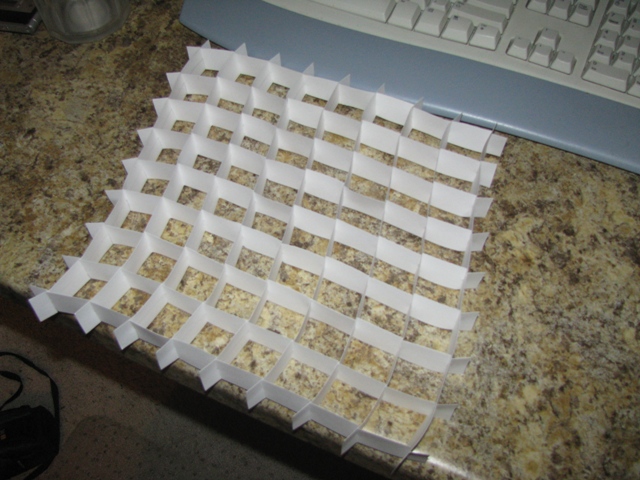
Finally, I made a grid out of posterboard to help block the light from one square from leaking to another square.
WEEK 15 SUMMARY Accomplishments: This week I worked a lot on the packaging. I also got all the routings for sampling and debouncing the imputs working. Weekly Work Total: 27 Project Work Total: 234
Week 16
April 26, 2009(9 hours): We all met today again. John let me know that it would be nice to have a flag that gets set when an event (piece up or down) occures on the board. I created a function that checks for these events that is run from the timer ISR.
I was able to get it to work except that row 0 repeats events. For example, if you place a piece on a square in row 1, the Pieceplaced struct is filled with the row and column, but when you place a piece on row 0 it repeats this and so the program interpretes it al placing a
piece down repeatedly. We tried a lot of different things(saving to a different varialbe for the previous state, changing the order and array size) but nothing worked. In order to narrow the problem down I wrote a small program that just prints the state of row 0 every time the
timer ISR runs, and it shows that there are no problems with the hardware. I wasn't able to get this resolved yet. I also worked on the hardware. I got the brackets for the LED timers mounted and the LED timer circuit boards mounted. I helped Matt make cables for these circuits.
I also got the microcontroller board mounted.
April 27, 2009(6 hours): I worked on getting the rest of the project mounted in the box. I also mounted a gromet in the bottom of the case to allow the power cables to pass through.
I also got all the capicators soldered on the main controller board the the touch sensor inputs (10nF). We worked on software again and we were finally able to figure out
what was wrong in the reed switch matric scanning function. After experimenting and finding that we would debounce the switches perfectly if we did it in main we were getting ready to move the code there when John noticed that I was passing global variables into my functions
and calling them the same thing inside the function. After we fixed this it worked perfectly. After we had this working we decided to demonstrate our PSSCs to Karl. We showed him, but we had a few problems with the sensitivity of the touch sensor inputs. I will change the 10nF
to 4.7nF and see if this helps. Karl wants up to use a wall wart to power our project instead of the benchtop power supply and we were able to get a 9V 3A power supply from Chuck.
April 28, 2009(6 hours): I conntected and tested the 9V 3A wall wart powering the chess board. It worked fine for a little while, but it caused the LDO to get very hot and then the board started acting funny.
The LEDs weren't lighting up correctly. I think the LDO was getting too hot and then dropping out. I quickly shut it off and reverted back to using the benchtop powersupply set to 6V. After switching back everything worked fine.
We will need to either get a 6V wall wart of just use the benchtop powersupply. I replaced the touch sensor capicators with 4.7 nF and it made the touch sensors perfect. They respond when you touch them but don't false detect hovering fingers or hands.
After I made the change I assembled the case.
We demonstrated our project for Professor Meyer in the senior design lab and everything ran perfectly.
After I finished assembling the board Hussain filmed the PSSC demo video which John and Matt then edited. I posted it on youtube:
May 1, 2009(3 hours): John, Hussain, and I gave our demo to the ECE 362 class. They seemed to like it. We also worked on revising our homework files for the final report.
May 2, 2009(3 hours): I met with Hussain John and we worked on the final report. Hussain and John revised the code and took screenshots of the schematics while I compiled it all together.
WEEK 16 SUMMARY Accomplishments: This week we got the reed switch matrix scanning problem fixed, finished the packaging, and demonstrated a completly working and integrated project! Weekly Work Total: 27 Project Work Total: 261