Tom Bottonari's Lab Notebook
Week 01
August 22, 2007 (3 hours):
We met as a team after class to research the feasibility of our original
project idea. Originally, we had hoped to create a version of the game Guitar
Hero using a real guitar, which would be used as a tool for teaching people how
to play guitar. We had hoped that we would be able to use signal processing to
achieve this goal, but after extensive research we concluded that this would
prove to be far too difficult given the amount of time that we have.
August 23, 2007 (5 hours):
With homework one (preliminary project proposal) due tomorrow, we began
thinking of other ways to determine which note was played other than digital
signal processing. We came up with a way of treating the physical guitar as a
circuit, capitalizing on the fact that the guitar strings were conductive and
the frets of the guitar were metal. We thought that maybe we could apply a
small voltage to each string and connect a wire from each fret to the micro,
thus when a fret was held down we would see a nominal voltage as an input to
the micro. However, we could not surmise a good way to determine if the note
was actually strummed. While we were determining methods to solve this problem
we noticed that all six strings are shorted due to the bridge being metal, and
decided to ditch the idea alltogether.
At this point we had three backup ideas (one of which was a spinoff of the
original). Our first idea was to use a MIDI keyboard instead of a guitar and
make a game that teaches someone to play piano. This was based on the idea that
it would be much easier to parse the MIDI format than process the signal of the
guitar.
Our second idea was to make it possible to operate such home appliances as an
oven remotely via sending a text message (and it returning a message when your
food is done).
Our final idea was to make an interactive poker table that could determine your
hole cards (in the case of Texas Holdem') via image processing, and keep track
of in-game statistics such as chip stacks using force transducers to weigh each
players chip stacks. Each person would have their own LCD display informing
them of the given bet and everybody's chip count. There would also be an option
to calculate hand odds based on everybody's hole cards as a learning mechanism
(would update throughout the game).
All three ideas were submitted for our preliminary project proposal.
WEEK 01 SUMMARY
Accomplishments: Determined our original idea was not
feasible, and submitted preliminary project proposal.
Weekly Work Total: 8 hours
Project Work Total: 8 hours
Week 02
August 28, 2007 (4 hours):
We met as a team to not only finalize our decision for our project, but also to
formulate our PSSC's for our presentation in class on 8/29/07. We went back and
forth between the piano idea and the poker table idea, but after much deliberation
and reading through some of the feedback we received from Proffessor Meyer and
the TAs, we decided to stick with the piano idea. Check out our PSSCs!
August 29, 2007 (3 hours):
I worked individually on designing our group website and setup everybody's
notebooks. There is information such a background information about ourselves,
documents relating to our project, everybody's notebooks, and pictures.
August 30, 2007 (4 hours):
We met as a team to tweak our PSSCs as well as finish the final project
proposal. Now that we had narrowed our project down to one idea, we could
finally focus solely on it and get our ideas organized. Some of the features
that we wanted to employ are as follows:
- We wanted our display to appear similar to Guitar Hero, in the sense that a
bar (of length corresponding to length the note should be pressed) scrolls down
the display above the appropriate key and the user presses the key until the
bar is finished scrolling.
- The game would be stand alone, and have capability of loading new MIDI
keyboard tracks via USB and generating the bar display on the fly.
- We will output the sound as long as the user is playing it correctly,
otherwise a negative sound will play.
- A running tally of your score will be displayed, as well as how many
consecutive notes you have played without error.
- If time allows, we will add a composing feature that allows you to record
your own MIDI tracks.
To see more details...Here is our
Final Project Proposal (HW2)
WEEK 02 SUMMARY
Accomplishments: PSSC and project proposal finalized.
Weekly Work Total: 11 hours
Project Work Total: 19 hours
Week 03
September 4, 2007 (2 hours):
We met as a group to begin discussing what kind of features we need to look at when choosing
a microprocessor, as well as how we plan to display our game. We decided that with the main
factor in choosing our micro will be graphics processing. We plan on using external flash
memory to store graphics and MIDI files, but we need to make sure we have enough SRAM on our
micro to support video and audio buffering. We probably need at least 4 MB of external flash,
and must make sure our micro has PWM support as well as a few ATD pins (at least two). We plan
on using USB data transmission to load MIDI tracks onto the device, so it would be nice if we
can find a micro with built-in compatibility. However, this is not a must. For the time being,
we plan on using VGA for our display. If this proves to be difficult, we will switch to LCD.
September 5, 2007 (3 hour):
I spent some time on my own researching VGA output to try to get a feel for how feasible it
would be. Curtis has been doing a good job researching parts, so I've been trying to keep up
with how we are going to actually implement them, since I am the lone Computer Engineer of our
group. We found some decently priced VGA computer monitors online and the evaluation board that
Curtis found actually has VGA output built in to it. The reason we want to stick with a VGA monitor
rather than an LCD screen is that we would like for the user to be able to translate what he/she is
seeing to the keyboard fairly easily and LCD screens are not available in very large sizes.
WEEK 03 SUMMARY
Accomplishments: Gained a better understanding for what parts we will need and
what lies ahead of us as far as interfacing those parts
Weekly Work Total: 5 hours
Project Work Total: 24 hours
Week 04
September 9, 2007 (3 hours):
Me and Curtis met in the lab about an hour and a half before meeting with the Bryan and Vik to do some
research on the Altera development board and whether it would suit our needs. We think it would be a good
fit for us and are trying to get one from Chuck as soon as possible so that we can begin writing software.
After meeting with Bryan and Vik, we discussed the design specifications homework due on Friday and
delegated tasks out to people as follows:
Bryan - Hardware block diagram
Curtis - Pick out a Microprocessor/Development Board
Tom - Software Flowchart/Block diagram
Vik - Power Supply design, monitor research
September 14, 2007 (2 hours):
We met as a group in the lab to finish researching Design Constraint Analysis details such as
final part numbers, prices, and current sinking/sourcing capabilities for the microprocessor.
Most of our Design Constraint Analysis homework that is due today has been completed, we just
had to fill in some final design values, proofread what Bryan had wrote, and submit. One thing
we are skeptical of is our ability to load a song from a USB stick into memory (whether it be
Flash or SDRAM). We included a USB receiver in our design however, for the time being. Also,
Vik brought to our attention a computer monitor that he found that would work very well for
our project. It is a widescreen 19" flat panel, with built in speakers for only $140
(Click to check it out). This would work very well because we could use thebuilt in speakers
and it would be small enough that it could rest on the music tray of the keyboard.
WEEK 04 SUMMARY
Accomplishments: Picked out all of our parts and submitted Design Specifications Homework
Weekly Work Total: 5 hours
Project Work Total: 29 hours
Week 05
September 17, 2007 (3 hours):
Today I did some work alone doing some research and adding some things to our webpage. Our
"Who We Are" section was not completed earlier, so I finished it off and then moved on to
more pressing issues. We are going to meet tonight to assign tasks such as VGA interface,
MIDI interpretation, and audio output. I worked for a while drawing out a rough flowchart
and psuedocode of how our game will run so that I could get an idea of what we're capable of
doing and what kind of graphics we will need to be able to produce. The first main task I
came accross was interpretting the MIDI formatted files. I found
this site to be
particularly helpful. Curtis got our development board today and has started experimenting
with it, so we should have a good idea of our graphics capabilities within the next few days.
September 17, 2007 (3 hours):
Met with Curtis and Bryan to discuss some issues that we felt we were a little behind on.
We still feel like there is much of this project that we have not planned out yet, so we
decided that we need to start working on our schematic as soon as possible because that
would serve as a good base. It is apparent that we will need to keep software (the micro)
and hardware (the FPGA) separate as we progress, so we defined the following I/O for
communication:
Input to microprocessor software:
1. MIDI Input from keypbard (through optical isolator)
2. Stored MIDI data from flash
Output from micro to FPGA:
1. Note and duration from MIDI for note bars
2. Tempo from MIDI and from potentiometer
3. Note played on keyboard
4. Score, song title, general game info
Hardware input:
1. All outputs from micro listed above.
2. Stored images (title, song selection, keyboard database)
Some other parts that we decided would be valuable additions were an optical isolator for
the MIDI input to the micro, and a MIDI jack mounted on our board so that a MIDI wire can
be easily connected. In the next few days, Curtis and Bryan are going to work on parsing
the MIDI input, while me and Vik work on outputting our display to a VGA monitor on our
development board. Furthermore, Curtis is attempting to locate a MIDI synthesizer that will
output audio from MIDI input.
September 18, 2007 (3 hours):
Today I went to the lab alone to brush up on my VHDL skills as well as read through the
tutorials and user manual for the Altera DE2 development board and Quartus II VHDL development
software. Vik met up with me an hour or so in and we continued going over documents and
tutorials. Some notable things that I found, were some information on schematics that are
used on our development board that we can use in our PCB design. For example, if you look at
Figure 4.11 on page 38 of the Altera DE2 User's Manual
there is a good VGA circuit schematic. Also, referencing pages 49-53 of the same manual outlines
schematics for SRAM/SDRAM/FLASH. On top of this, I also noticed a full schematic of our development board on the CD that comes with it.
September 18, 2007 (4 hours):
After class we all met down in the lab to continue working. We began the meeting looking through
the schematics in the above link and began determining which components we would need in our
design. After a while it became apparent that we didn't all need to be working on this, so Bryan
and Vik continued work on the schematic while I went back to working on VGA output and Curtis
continued research on parsing MIDI files. I found some some compiled (.sof) Demo files online and loaded one on our FPGA that displayed a moving
block that bounced up and down the screen. This gave us hope, as the falling block is similar
to what we would need to output in a simplistic sense. Unfortunately, none of the sample code
that came on the Altera CD is in VHDL, but rather in verilog (which I am unfamiliar with). I
will have to find some sample code online in VHDL so I can start learning from it and coding
my own outputs.
September 19, 2007 (3 hours):
We all met in the lab to continue work that we all started yesterday. The theme for today, though
has been progress, which is good. Curtis is now able to decypher MIDI files, and we feel very
confident about our ability to parse a MIDI file, and I finally got an image that I loaded into
SRAM to display on a monitor. This is no where near as complicated making our own graphics, but
since we will need to use a background image for the title screens, it is a good sign. I found
a good VHDL source code file that I am using to learn from, and I e-mailed someone else about
obtaining the source code for the moving block program that I described yesterday, as that is
somewhat similar to what we will be outputting. Also, Professor Johnson is contacting someone
he knows at Altera so that we can ask them about the best method for programming our chip on our
PCB.
September 20, 2007 (1 hours):
We all worked independantly today to get datasheets, prices, and dimensions for all of our parts
and put them into an Excel Spreadsheet for
easy access in the future. The main need for this was to organize all of our parts and to get an
idea of how big our PCB will be. This spreadsheet also proved to be useful in beginning our full
schematic, and ordering all of our parts.
September 21, 2007 (1 hours):
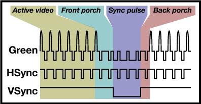
I went to the lab alone today between classes to do some more reading on VGA programming, and found
a great website that helped
explain VGA timing signals. This picture shows the correct order that the signals should be sent.
For more information, see aforementioned website detailing the meaning of Front/Back portch and
sync pulses:
WEEK 05 SUMMARY
Accomplishments: Turned in our Packaging Design Homework (Homework 4) and gained a better understanding about how to accomplish VGA output.
Weekly Work Total: 18 hours
Project Work Total: 47 hours
Week 06
September 24, 2007 (1 hours):
We met today in the lab to basically organize the rest of the week. We decided to have fixed meeting
times twice a week: Mondays at 3:30 and Wednesdays at 10:30. These are meant to ensure that everyone
is staying on track, and other meetings will be called as needed. This is how we are currently orgainized:
- Curtis is researching MIDI file parsing and accepting MIDI input
- I am researching VGA output
- Vik and Bryan are getting together our parts and schematics
Once Curtis and I have figured out the background information on our appropriate topics, Vik will
merge with me and Bryan will merge with Curtis, helping us code. Furthermore, while we were together, we
began ordering parts.
September 27, 2007 (4 hours):
Today I did work alone, with Bryan, and met with Professor Johnson. I began by discussing some issues
that we had not yet settled with Professor Johnson. The first thing that I wanted to discuss with him
was whether or not it would be possible to read/write to SRAM with a single port SRAM chip. We were
worried that since we are reading a new pixel from RAM about once every .0739 ms we might run into
traffic issues on the bidirectional data bus (not having enough time to write in between reads). If
we were to use a dual port chip, this would alleviate the problem, but would essentially almost double
our pins used (which was somewhat of a constraint already). Professor had a very good idea that would
solve our problem. This came down to either writing exclusively when the VGA output is in the vertical
blanking period (down time just after complete screen refresh), or double buffering. If we were to go
the double buffering route, we would have twice the needed RAM and basically read from block while the
other is being updated, and then switching on the next refresh. Both methods eleminate the need for
dual port data buses, since we would never be reading and writing at the same time. Basically, we will
need to calculate if we can update the whole screen in the alotted blanking interval, and choose
appropriately.
When Bryan and I met we came to the decision that we should definitely store color lookup values in RAM
instead of the actual 24 bit color values. Basically there will be a 4-8 bit lookup value that will be
read from memory and decoded to its actual RGB values and sent to the DAC. This will save us alot of memory
and I/O pins. Bryan and I are in charge of completing the schematic for the VGA, SRAM, DAC, and FPGA
circuits for the homework that is due Friday, so we also spent some time mapping out which pins will need
to go where and what other components (resistors, capacitors, etc.) will need to be added. The only thing
we have left to determine is if we will double buffer, or single buffer. One problem we found was that
with the given pixel clock (40 MHz) we will not be able to read data from SRAM fast enough. We will need
a new pixel color value about once every 25 ns, but the data access time of the SRAM chip is about 50 ns.
However, the way we are getting around this is by using a 16 bit wide data bus, thus grabbing 3 pixel
values (if we use a 5 bit color identifier), and essentially tripling our throughput.
September 28, 2007 (3 hours):
I finished my calculations and came up with the following numbers:
The total amt of time during the vertical blanking period = 0.739 ms
The total amt of time to refresh the whole screen once = 0.0167 s
Our SRAM that we have picked out is 512k x 8, and has a data access time of 12 ns. This means that it
will take about 12 ns to write each 8-bit pixel color lookup identifier:
12ns x 800 x 600 = .00576 s
As you can see, this is too much time to do our writing in the vertical blanking period, so we will need
to double buffer (which we should have plenty of time for since we have the entire duration of a screen
refresh). The rest of my work done today was spent on building our schematic that is due Friday.
September 28, 2007 (9 hours):
Me, Bryan, and Vik met in lab after class to finish our final schematic that is due tomorrow. I mostly
focused on the FPGA circuit and the SRAM circuit. The SRAM circuit was mostly dependent on how many
pins of the FPGA would be available (determine whether we would double buffer or try to write everything
during the vertical blanking period). We feel that we should be able to get away with writing only during
this blanking period unless we have to rewrite the entire screen (which will only happen in the transition
from main menu to gameplay). After creating our FPGA schematic part (all 240 pins!) we determined that
unless we get rid of USB capability (which is an option since it is not one of our PSSCs) we will not have
enough pins to double buffer. Therefore, the decision was made to single buffer unless USB gets removed at
a later date. Part of the process of creating the FPGA part also included learning exactly what each pin of
the part is used for, and what it needs to be tied to. This was a time consuming process as you can see from
the amount of time spent in the lab today. After all of the hard work,
here is our Homework 5
and
here is our final schematic!
WEEK 06 SUMMARY
Accomplishments: We finished our Homework 5 and Final Schematic
Weekly Work Total: 17 hours
Project Work Total: 64 hours
Week 07
October 1, 2007 (6 hours):
We all met in the lab to begin work on our PCB layout. Since this is one of the most important stages of our
project, we are really trying to make sure that we do it right the first time. In order to use our schematic
to generate the basic layout in ORCAD, we had to spend some time reformatting our schematic to match what they
wanted, and in doing so, we also organized the pins on the FPGA so that all of the appropriate circuits were
in the same vascinity as one another. Along the way, a few decisions were finally made. We decided to completely
get rid of our USB controller circuit, since this was not one of our PSSCs and it will merely add complexity to
our already complex project, as well as take up I/O pins. However, now that we had extra I/O pins we had to make
a final decision on whether we would single or double buffer (as you can see in my previous posts we have gone
back and forth on this issue). In the end we decided to single buffer for a few reasons. If we double buffered,
the programming would be a little more straight forward, but it would leave us with virtually no I/O pins to debug
or to use as a backup if something goes wrong. Plus we feel fairly certain that we should be able to manage writing
to SRAM in the vertical blanking period (or even the horizontal blanking period if need be). The data traffic
management may be a little more complex, but the added benefit of having the extra I/O pins is worth the labor,
not to mention the fact that it will be hard enough to get our 240 pin FPGA routed on two layer PCB board. An
extra SRAM chip would just be added complexity. Dr. Meyer expressed some concern over this matter, and we are
going to meet with him tomorrow to discuss that issue in further detail.
October 2, 2007 (5 hours):
Curtis, Bryan, and I met with Professor Meyer to discuss the feasibility of putting our circuit on a
two layer board and, with the input of Chuck as well, we ultimately came to the decision of using a four
layer board. These are about twice as expensive ($66 or so), but the added benefit is definitely worth it.
After meeting with Meyer, we received an e-mail from our contact at Altera informing us that there is no
programming compatability with the FPGA over RS-232, which we had previously planned on. This news led us
to doing some more research on their site, and we discovered that you can buy their "USB Blaster" connector
(which is used to program the micro on the development board). This was very good news because we had assumed
that we would have to recreate their "USB Blaster" circuit ourselves (which looking at their schematics, looked
like a daunting task). The image below shows how the USB cable plugs into the connector, which plugs into the
header. In locating this connector, we also stumbled across another part that would add to the simplicity of
our design. Altera makes a "Serial Configuration Device" that basically is a large chunk of flash that has
a certain amount dedicated to the system boot. This device only requires four FPGA I/O pins, since it is all
serial, (as opposed to the 35 Flash pins) so we quickly decided to do away with our Flash chip and use this
device. This required an overhaul of our schematic, as well as some additional timing considerations, since
the serial flash is much slower than that in parallel. Therefore, we decided to use the removed Flash pins to
put a second SRAM chip that will store only "sprites", or preconfigured images or text images that will be
loaded from Flash upon bootup. Since they will be stored in SRAM, we will have easy access to them.

October 2, 2007 (3 hours):
At this point I did one final run through of the whole schematic with Curtis, and found a few more mistakes.
It seems like every time we think the schematic is done, there are a few things we have to change. Curtis
started making PCB footprints while I finalized as much of the schematic as possible. We still have to add
some bypass capacitors, but as of now most of the schematic is completed and ready for layout. After class
tomorrow we plan on clearing up our questions about if we are using enough bypass caps, as well as if we
are creating the PCB footprints correctly.
October 3, 2007 (9 hours):
We spent all day in the lab working on our PCB layout. Throughout the process of checking over our schematic,
we realized that we forgot to add a power switch to our circuit. I don't know how we missed something like
that...but I'm glad we caught it. Also, we took this opportunity to route some important signals to headers
and test points onto our schematic. The signals that we decided to grab other than I/O were the two SRAM data
buses (so that we can check the data bytes accessed), the regulated power sources, and audio out. A large
portion of this meeting was dedicated to both collecting part footprints and creating footprints for parts
that we could not find. After many hours of carefully creating and collecting parts, we finally got our nets
list imported into orcad layout, and generated our rats nest, leaving the daunting task of routing our PCB
for tomorrow.
October 4/5, 2007 (13 hours):
I wish I could say more about what we did today, but the vast majority of this meeting was spent dealing with
OrCad Layout (and its illogical behaviour) and routing our PCB. You'll have to check out our preliminary PCB
Design to see what we've been doing for the past week!
WEEK 07 SUMMARY
Accomplishments: Finished Preliminary PCB design
Weekly Work Total: 36 hours
Project Work Total: 100 hours
Week 08
October 9, 2007 (1 hours):
Curtis, Vik, and I met in the lab to print off our schematics and PCB layout, as well as organize our
thoughts for our 10 minute design review tomorrow.
October 10, 2007 (7 hours):
I went to office hours today to try to clear up some things with our PCB. We weren't sure that our vias to
the ground/power planes were connecting properly because the rats nest for ground/power was not disappearing,
but we then learned that using free vias you can specify the net that you would like to attach to. Unfortunately
not too many people have had experience with 4-layer boards, but it seems that it is finally connected correctly.
I spent some time rearranging our bypass capacitors around our FPGA (which took longer than expected since there
are 30+ of them and I spent most of the time trying to get our vias connected to ground), and started spacing our
traces farther apart. This is not an easy task, because even though our board was pretty tight when the traces
were spaced at 9 mils, we wanted them to be spaced 12 mils apart. This means getting creative with alot of traces
and vias, and will take a while to clean up. However, in the end the time spent now will be worth not losing a
trace after it is fabricated. A few other adjustments were made along the way such as moving the MIDI chip closer
to the audio output jack to minimize noise on the analog audio traces. After a few hours Bryan and Curtis showed
up and after talking, we decided that although it felt neccessary to have all four of us working full boar on our
PCB layout, we were getting very behind in software. Therefore, after our design review I am focusing solely on
software so that we can be making progress on both fronts.
October 10, 2007 (3 hours):
After leaving the lab, I spent an hour or so creating a software flowchart and working on the software design portion
of our design review. Then I went to the lab to meet up with Bryan since we were both discussing the PCB layout.
We created the slides for our presentation and divied up who was going to talk about what. Then I spent some time
going through my slides and jotting down some notes of what I wanted to talk about.
October 11, 2007 (1 hours):
We met in the lab today before our presentation to assemble all of our slides into one file and print everything
(slides, schematics, and PCB). This was more of a challenge than expected because we could not find a printer for
the 11 x 17 page schematics, and the printer in the lab was being occupied by another group and moving really
slowly. However, we got everything printed in the nick of time! Check out our design review presentation!.
October 12, 2007 (3 hours):
I went to lab after reviewing team 3's presentation to start laying out software considerations. However, before
beginning this, I wanted to make sure that everyone else had a clear idea of what needed to be changed on our PCB.
I made the following list of things that I think should be changed before submission:
- Update our netlist (we have made some changes to the schematic)
- Move the MIDI synth chip closer to the Audio Jack to minimize noise on analog traces
- Reorganize ring of bypass capacitors around the FPGA (right now there are none on the left side
- Make sure all traces are 12 mils apart (it's ok to converge at the pins to 9 mils apart, but avoid this for the
majority of the trace
- Make sure the 3 bulk capacitors are near the voltage regulators and not mixed in with the bypass capacitors
- Add the headers for the address busses on the two SRAM chips
- Add a pushbutton on two I/O pins for a soft/hard software reset
- Finish adding power/ground vias
- Add power plane copper pours
- Remove 40 MHz oscillator
- Make sure we have bypass capacitors on all peripheral chips (not just FPGA)
We want to have this completed by Wednesday evening so that we can review it with Professor Meyer in his office hours
on Thursday and make the appropriate adjustments for Friday.
After finishing the list, I began mapping out the software. I've written psuedocode for displaying our output on the
monitor, and began thinking about our color lookup table. I began thinking of what colors we will actually want to
use when it occured to me that it might be worth it to just not use a DAC at all and be limited to 8 colors. This would
leave us with the option of Black, White, Red, Green, Blue, Cyan, Yellow, and Magenta. Perhaps it is too late in the
design period to make this change, but I think we could easily construct our whole game with these colors. I will talk
about it with the guys sometime soon. I began thinking about the code involved in writing to our video buffer and began
to see how complex the timing will have to be since we can't read and write at the same time, so for now I'm going to
focus on getting the reading to work and wait until one of the other guys can help me work out the timing. Another
design consideration that I realized today was the way in which the processor and FPGA communicate. I think up until
now we had all just assumed that they can communicate internally since they are in the same chip, but this may have
been somewhat of an oversight. As I thought about it more, I began thinking that we will have to tell the processor
to output a signal on an I/O pin and then recieve it on another I/O pin but tell the FPGA to read the latter pin. This
is not a huge deal since we have plenty of I/O left over, it will just require more traces. Again, I will discuss this
issue with the guys next time I see them.
WEEK 08 SUMMARY
Accomplishments: We presented our project to the staff and two other teams and progressed in our
PCB layout
Weekly Work Total: 15 hours
Project Work Total: 115 hours
Week 09
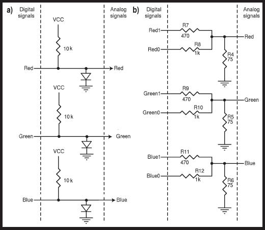
October 13, 2007 (3 hours):
I went to the lab to read through some tutorials regarding the Quartus II software that came with the Altera Development
Board. Curtis said he saw somewhere that it is possible to communicate internally between the microprocessor and the FPGA,
so I am currently researching how exactly that works. To answer another question raised in my previous post, we are currently
planning on keeping our DAC in the circuit (since we have already done most of the work), and using the circuit on the right
in the picture below as a "Plan B". This circuit is basically a homemade DAC that will allow for 64 colors.
October 14, 2007 (3 hours):
I spent some more time finishing up some research on how our code will be implimented and came up with some
answers as well as some more questions. I think that I may have figured out how exactly the FPGA and microprocessor
communicate. It looks like within the Quartus II software you can use the SOPC builder tool to add a communication
bus module that communicates with the processor. I'm still a little unclear on the topic though, so I plan on going
to Professor Johnson's office hours tomorrow to see how much experience he has on the subject. While I'm there
I also need to ask him how exactly to declare which I/O pins are which (since this can not be done in the VHDL
code). At this point, I feel pretty comfortable in how our software will be layed out, and I'm ready to try
loading some test code onto the development board. We tried this early in the semester and had trouble loading
the NIOS C-code, so I'll have to determine what we were doing wrong. The rest my time this evening was spent
doing just that.
October 15, 2007 (5 hours):
I met with Professor Johnson this morning and he suggested a few different ways of communicating between the
FPGA and processor. He didn't know the answer off hand, but we looked through some documents and the two main
solutions appeared to be Memory Mapped I/O, and user defined processor instructions. I haven't had
time to read further on these two interfaces, but it looks like it will be possible to do this internally, so
that should save us time on the PCB. After this, I went to the lab to try to figure out how to completely
compile and load a program on the development board from start to finish. This proved to be alot more complicated
than previously anticipated. I went through about 3 hours of tutorials and have a basic idea of how to create
the NIOS embedded system, as well as how to add peripherals such as memory interfaces and parallel I/O. There
is a laundry list of configuration settings that must be set before the two programs (FPGA and processor code)
can actually be loaded, such as pin assignments, etc. I finally got to the end of the tutorials and was able
to load the FPGA code, but when trying to load the NIOS code I received an error stating:
Using cable
"USB-Blaster [USB-0]", device 1, instance 0x00
Resetting and pausing target processor: FAILED
Leaving target processor paused
After researching this error, it appears that we do not have the full NIOS liscence loaded on our computer
and there is a glitch in the evaluation version that we have that is causing the error. I will need to make
sure we have the correct liscence loaded tomorrow because Chuck has already left for the day.
October 16, 2007 (2 hours):
After talking with Chuck and Professor Johnson, we decided that the problem was that we were using an old
version of the Quartus II / NIOS II software. I am currently downloading version 7.2 for both packages
and after Chuck updates the liscencing information we are hoping that the error is fixed.
October 17, 2007 (4 hours):
Unfortunately, the aforementioned proposed solution in my previous entry did not fix our situation.
I really think that for some reason our licensing information is not set correctly, because whenever
we compile our FPGA design using an embedded processor it compiles into projectname_time_limited.sof,
which essentially means that we do not have the full NIOS license and once you untether the board
from the computer, the code will only work for an hour. However, even with the time_limited file
we should be able to load the code onto the chip. I talked to Professor Johnson and he took a look
at our license and said that it looked ok, so he is going to install Quartus II and NIOS II on the
linux machines and give our group account access to the software. We are hoping that this works,
but are moving ahead with programming, because too much time has been wasted on this. Needless to
say, most of the time today was spent going through Altera tutorials and reading through forums,
trying to figure out why the NIOS II software will not let us load C code onto the processor. Many
people have had the exact same problem, but the few solutions I have come accross have not helped
us.
October 19, 2007 (8 hours):
I spent all of today focusing on VGA output with Vik instead of worrying about our issues with the NIOS II
software. I've done enough research on how to output to a monitor that I could pretty much write the
code in my sleep, so after only an hour or two I had the code written and had the rest of the day
to debug and work with configuring the FPGA properly. The first step after the basic code was written
involved figuring out how to declare the proper pins in Quartus II. There is a window called the "PIN
Planner" that allows you to assign each signal in the VHDL code to a different pin. This involved some
reading of the Altera DE2 board schematics to make sure that we were assigning the correct signals to
the correct pins so they could be routed to the respective peripheral components such as the DAC and
the VGA connector. After this came the debugging. Although I am the only one on our team that knows
VHDL, Vik was very helpful in debugging our design, which was good because since it takes almost a
minute to compile the design, it makes the guess and check method fairly time consuming. However,
since we were trying to make a color appear on a VGA monitor, I chose not debug in simulation, but just
to debug off of the actual chip. This was mostly due to the fact that I only know how to simulate in
ModelSim, and have had enough of trying to figure out how to do things in Altera's software. The first
thing we did was simulate our color code (which is fed to a lookup table in our code) to 8 of the 17
switches on the front of the board. This way we could manually change the color output. In order to
make sure we had the pins configured correctly, we mapped each bit of the color code to a corresponding
LED that is also on the development board. Everything appeared to be working fine, but to our greatest
surprise it did not work on the first try! (insert sarcasm). We then attempted debugging by first
setting our digital Red signal out to the LEDs. After a little debugging, we acheived this output
but still saw nothing on the monitor. The next step was making sure the clock was correct. We were
able to see the 25 MHz pixel clock, but it was not by any means a square wave. We assumed this was
due to attenuation and that the signal that the DAC was receiving was correct. We noticed that when
we hit the reset button (programmed to one of the pushbuttons of the board) the monitor momentarily
received a signal (although just a black screen). After looking through our code for a while, we
realized we were using our blanking signal as active high instead of active low, and this is why
we couldn't see any color. After changing this, as well as hours of debugging (far too much to
describe in detail here), we finally got a single color output to the monitor based on our color
code given by the input switches of the board. The next step is to save the pixel codes to SRAM
and be able to read everything off of memory.


WEEK 09 SUMMARY
Accomplishments: We finished our PCB layout and I am now able to output to a
computer monitor via VGA
Weekly Work Total: 25 hours
Project Work Total: 140 hours
Week 10
October 21, 2007 (3 hours):
Vik and I spent a few hours in the lab working on interfacing our VGA output code with the SRAM chip.
We would like to be able to read all of the respective color codes from memory rather than the input
switches. This brings up quite a few timing implications that must be worked through, so alot of
thought must be put into it before we write any code. We decided we want to output the top half of
the screen blue and the bottom half as green. Therefore, before we read any of the values to the
monitor, we will actually have to write each value into the SRAM. Since the data access (read/write)
times of the SRAM chip are 10-12 ns, we have to make sure that we do not change the address values
until it has completed the read/write. Fortunately, our 80 MHz clock has a period of 12.5 ns, so we
should just be able to write on each clock edge. However, our previous code was executed using the
50 MHz clock that the development board has on it, so in an effort to not reinvent the wheel down
the road, we are going to wire up an external 80 MHz oscillator circuit and input it into the development
board. That way, we will not have to change our code much when we impliment this on our actual design.
October 22, 2007 (2 hours):
We are submitting our PCB design today at 4:00, even though it was supposed to be due last Friday
(we had to completely reroute our board). While Bryan was finishing that up, I finished all of the
documentation that accompanies the submission, as well as found an enclosure that would suit our
board.
October 23, 2007 (8 hours):
I did alot of work today both by myself and in discussion with Curtis. The first thing I noticed
was that our method of interfacing to the SRAM by brute force may be more complicated than expected.
I remembered doing the timing analysis for interfacing an microprocessor with an SRAM device in
ECE362 with all of the delay constants and began to get a headache. However, after referencing the
SRAM data sheet, I noticed two methods of interfacing were described, one being much easier to
think about than the other. If you look below, the timing diagrams for Addressed controlled read cycles
and OE/CE controlled read cycles are shown. As long as you keep CE/OE low (active low), you simply
have to change the address bus at the appropriate time and just worry about the address access time and
output hold time.

Unfortunately, the write cycles will be a bit more complicated (comparable to the OE/CE controlled
read cycle).
I spoke with Curtis about different methods of sending data corresponding to each bar on the screen
to the FPGA, and we came up with a few ideas. The first idea is keeping a map of the whole screen
(48 bits wide for each key and 100 bits deep corresponding to the vertical location). The top row
of bits will be updated based on the notes from the MIDI files, and, based on a certain timer, will
propagate down the screen until it reaches the keyboard at the bottom. Once the user presses the key
we will check how far away the bar is and grade them accordingly.
The other option is to dynamically create a variable for each bar, storing it's upper and lower bound
and checking it's location when it reaches the bottom. However, if at all possible we would like to
avoid memory allocation.
Much of the other time today was spent researching the best way to impliment our software, communicate
between the FPGA and processor, and making the TCSP for tomorrow. I tweaked my flowchart from the
design review and created a block diagram for the VHDL code, showing the different blocks of within
the hardware logic. From a top level perspective, the main code is a state machine, with each page
acting as a new state (start screen, select song screen, gameplay screen, and end song screen).
Basically, we are going to have to be very careful when implimenting our software, because timing
is incredibly crutial for us, especially since we are communicating between so many devices.
October 24, 2007 (8 hours):
Curtis and I met to discuss further the best way to handle the storing of note information and we
came up with a few more ideas. One idea we had was to just pass the FPGA a single vector containing
every key that should be pressed at that given time (48 bits wide). This would be easy, since the
MIDI format supplies you with the time instance when a key is pressed or released. Then, this
information will be stored in the SRAM location corresponding to the top row of the screen. While
we are reading from the first SRAM chip, we will read in each line of second SRAM to a buffer (starting
at the bottom) and then write the same line to the row below it, thus creating a propagation of all
of the bars down the screen. Another idea we had is simply limiting there to be a max of about 20
bars on the screen at once, and storing their location variables in memory and displaying them accordingly
this is more of a straightforward way to do it, but would require more overhead. After all of the talk
about software, we decided to make another attempt at getting the Nios processor working. This was
spawned by the thought that if we do not have the licensing to do so, then we would have to implement
every code block in VHDL. Professor Johnson had installed the software on the Linux machines so we
could give it a shot there, but this time we were receiving an error before we were even able to
attempt to run the code. After this failed effort, we went to talk to Professor Johnson in his office.
We again tried to run it from his office, and again there was an error. After heading back downstairs
Curtis wanted to try loading some software onto the Nios so that he could get the exact error and send
a message to Altera. However, by some stroke of a miracle, the code loaded successfully and the terminal
window said "Hello from Altera", as it was supposed to. We intend on testing a few more sets of sample
code that we have just to make sure everything is working correctly, but unfortunately had to leave.
However, regardless of whether the Nios was able to load, whenever we compile a project in the Quartus
software while using the embedded Nios processor, our build file is a "time_limited" file, which will
only work for an hour after untethering the board from the computer. As you might guess, this is
unacceptable for our project, so we still need to work out our licensing issues.
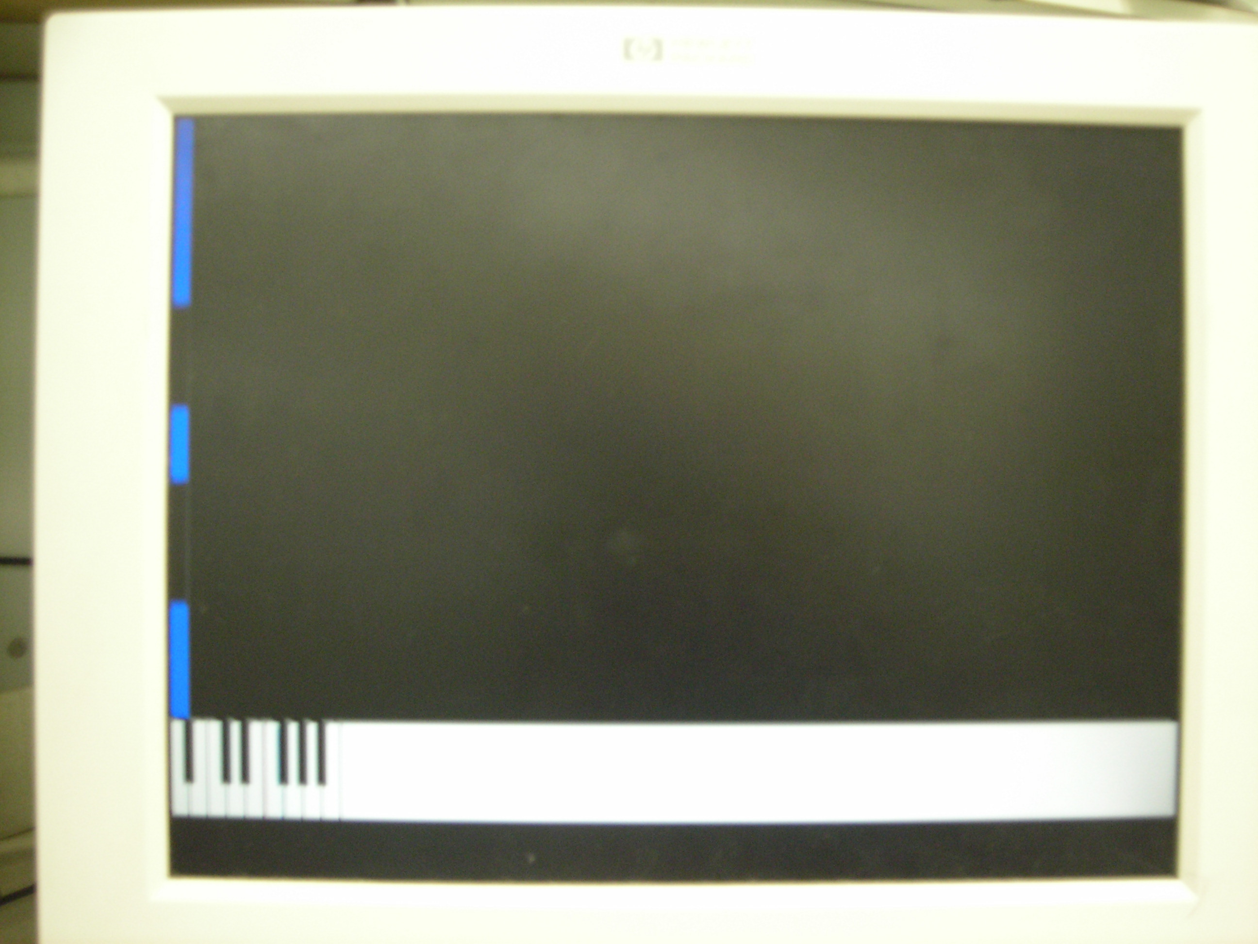
October 25, 2007 (10 hours):
Most of today was spent in the lab by myself working on the report that is due tomorrow.
Check it out! However, afterwards I spent a few hours
with Vik drawing out some text sprites and outputed them to the screen (see image below). We are still
testing in 640 x 480 resolution and have ordered an 80 MHz through-hole oscillator so that we can test
800 x 600 resolution with our development board. Also, I would rather program the reading and writing
to the SRAM chips using our 80 MHz clock (rather than the 50 MHz oscillator on our board) so that there
are no surprises when we switch to our PCB.


WEEK 10 SUMMARY
Accomplishments: We submitted our PCB layout, turned in our software design homework,
and got text sprites to output to the screen
Weekly Work Total: 31 hours
Project Work Total: 171 hours
Week 11
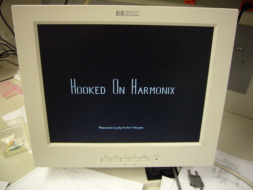
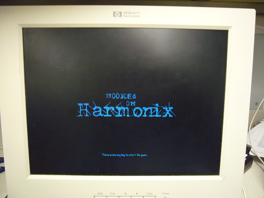
October 29, 2007 (7 hours):
I began working on our output control code block today. Basically it will determine what gets output to
our monitor based on where the user is in the game. For instance, when the board boots up, the text
"Hooked On Harmonix" shows up, with "Please press any key to start the game" under it (as seen in the
picture above). Bryan and Curtis are currently working on accepting MIDI input, so in the meantime I
am using one of the buttons on our development board as a key event. After this button is pressed, a
new screen shows up with an arrow that will toggle up or down (pointing to 5 different song names) based
on similar button input. Amazingly enough, this entire program (with all of the aforementioned text sprites)
uses about 2% of the total logic elements available on the FPGA on our development board. Since the FPGA
we are using on our PCB has half as many logic elements, this means it will be using 4% of the total logic
elements in that chip, which is much better than I had anticipated. Without crunching the numbers, part of
me thinks we might even be able to handle all of our video output within our VHDL code (thus phasing out
our SRAM chips). I will have a better idea with more testing, but every screen except for the gameplay
screen can definitely be done outside of SRAM.
October 30, 2007 (3 hours):
Curtis was able to achieve a clean digital signal yesterday on the oscilloscope from the MIDI out of our
keyboard after assembling our MIDI input circuit on a breadboard. I began analyzing the signal this morning
and trying to make sense of it. I found lots of documentation outlining the standard MIDI message packet
format, but this did not seem to match what we were seeing. However, after lots of testing, I think I
understand how it is displaying the information. To begin with, it should be mentioned that MIDI devices
can relay information in a few different ways. The first is sending a note-on packet with the note number
and volume of the note (intensity of the key pressed), as well as the corresponding note-off packet with
similar information. All of the standard MIDI documentation pointed towards this method as being the standard.
However, another method (which our keyboard appears to be using) is simply sending the note pressed and a
volume associated with it when you want the note to turn on, and sending the same packet only with the volume
equal to zero when you want the note to turn off. We were having trouble matching the first byte with the
note pressed originally, but could definitely see the second byte go to zero when the note was released.
After some more testing, I finally realized that it was sending the least significant bit of the note value
byte first, so by looking at the waveform on the scope, it appears backwards. We are now pretty confident
with our ability to interpret this MIDI signal, but there are two things left that we haven't figured out.
When the keyboard is idle (there are no keys being pressed) there appears to be a strobe occuring at a
non-uniform rate. It is four pulses wide (32 ns per pulse) and does not appear to be at a steady frequency.
Our best guess right now is that it is just a strobe indicating what MIDI channel is currently being used.
Since the idle state is logic high, the four low pulses would correspond to Channel 1 of 16. However, we
have seen cases where the MIDI message packet occurs just after or just before this strobe, and it may
complicate the receiver that we will have to program. The second question we must get answered is why the
packet appears to be 19 bits long (it is supposed to be 2 bytes). We know one of these extra three bits is
to signify the beginning of a packet (dropping from idle '1' to '0' for one clock cycle), but do not yet
know where the other two come from (we assume they signify the end of packet in some way).
October 30, 2007 (3 hours):
I came back into lab today to look more into the MIDI format, and after talking to Bryan it seems that he
is getting different looking packets on the scope. This was very confusing, and Bryan decided to attempt
to use the logic analyzer to view the data. It was at this point where I decided to start coding the
MIDI receiver in VHDL and leave the MIDI formatting up to him. Since the pulse width of a MIDI bit is an
exact multiple of a pulse width of our system clock, our MIDI receiver would need to sample every 2560
pulses from our 80 MHz clock. I began coding as if we had access to our 80 MHz clock (even though the clock
on our development board was 50 MHz), and luckily shortly after Curtis was able to get the PLL working using
the SOPC builder tool in the Quartus II software, and transform our 50 MHz into 80 MHz. Tomorrow I plan on
testing the 800 x 600 resolution, now that we have access to an 80 MHz clock.
October 31, 2007 (2 hours):
Curtis and I began work interfacing the embedded processor with the FPGA. The interface we created allows
for use of the LCD on the devolopment board, as well as the flash memory and employs the use of the PLL
to achieve our 80 MHz clock. After a few attempts at remembering how to make a toplevel vhdl file, we
were able to link the vhdl code I had written and the code that the SOPC builder tool had generated for
our interface with the embedded system. Our 800 x 600 resolution has officially been tested now, and we
are currently in the process of loading a C file onto the embedded processor.
November 1, 2007 (7 hours):
Curtis is in charge of debugging our errors with loading the C file onto the processor, so in the mean
time I thought this would be a good chance to work more on the gameplay screen. I used the method of
just checking values of vcount and hcount (position on the monitor) and setting the color_code accordingly
in order to build the keyboard at the bottom of the screen. I think that will be faster than building the
actual sprite, plus it will save us some room. I just built the first octave, because if we decide we don't
have enough logic elements to dynamically create our screen, then we will have to create a keyboard sprite
and store it in SRAM, thus voiding everything I did to dynamically create it. After doing this I thought
for a while about how feasible it would be to create the scrolling bars "on-the-fly", and decided to try
to implement the method of having a simplified mapping of the whole screen for just one key. In this method,
we would have an array of 200 std_logic_vectors of length 87 (one bit for each key of a full keyboard).
Row 0 of the array will be continuously updated from the processor with which keys need to be pressed. Then,
every certain amount of clock cycles (given by a counter in hardware), each row of the array will propagate down
one row, thus creating a scrolling effect. While in the "gameplay" state, the screen will be constantly
checking values of this screen mapping and painting a certain color if a '1' is currently at the position
of the array corresponding to the position on the screen. For testing purposes, I made the value of row 0
equal to one of the pushbuttons on our board. After thinking through some pseudo-code and doing some
debugging, I was able to achieve a scrolling bar on the screen of however length I held down the pushbutton.
November 3, 2007 (8 hours):
Curtis, Bryan, and I worked in the lab today on some individual tasks, but we helped each other out alot.
Bryan spent most of his time doing starting soldering our PCB, while Curtis was still rigorously working
on getting functionality out of our processor (which has proved to be much more of a pain than anticipated).
I spent most of my time today increasing the functionality of the scrolling bars to every key on the full
88-key keyboard displayed on our screen. This was not as easy as I had hoped. As mentioned before, as the
monitor is scanning it is checking a bar-map of the whole playgrid to see if a bar line should be displayed
or not. This was easy to implement in the vertical sense, because I just made the number of rows equal to
half of the vertical dimension of the grid, so I could just divide vcount by 2. However, since the black
and white keys are different widths, and since the black keys can overlap the white keys, it was not this
easy in the horizontal direction. Therefore, after an hour or two of trying to come up with a clever way
to check each spot of the mapping and tie it to the actual position on the monitor, I just decided to
hardcode each pixel range as a certain key. This was quite time consuming and tedious, but I could find
no way around it, and it works!

WEEK 11 SUMMARY
Accomplishments: We turned in our Patent Liability homework, and I acheived scrolling
bars on our gameplay screen for every key!
Weekly Work Total: 30 hours
Project Work Total: 201 hours
Week 12
November 5, 2007 (9 hours):
Today I began working on the scoring system for our game. The first thing I did was simply look at the
first column and monitor the area around the top of the picture of the keyboard. If the button was
pressed when the bar was within a 5 pixel window of the top of the keyboard, the word "GOOD" would
appear under the keyboard. However, if the button was pressed when the bar was outside this region, or
if no button was pressed and the bar is 5 pixels below the top of the keyboard, the word "MISS" is
displayed. I attempted to increase this functionality to every key, but that was not initially
successful. With more pressing issues on our plate at the moment, I decided that I would think more
about increasing it to more keys later. However, the next thing that I added was a scoremeter on the
right side of the screen. This meter starts out half full and either increases or decreases depending
on the user's performance. It was about at this point that Curtis and I decided to attempt to run our
VHDL code with input from the processor. Curtis wrote a simple program that sent an 87 bit vector to
the VHDL, but when we compiled the project we noticed something startling. The compilation was taking
longer than usual, and when it finished we noticed that it was using 86% of the FPGA's logic elements
(as opposed to the previous 17%). This was not good, because our FPGA has half as many logic elements
as the FPGA on our development board. After a few hours of debugging, we narrowed it down to a few
lines that we know are causing the problem. The assignment of the 87 bit vector that he is passing me
to the top row of our bar-mapping matrix is causing the large jump in logic elements for some reason.
We tried writing the code different ways, but to no avail. It makes no sense to me why this would be
happening, so I will probably ask Professor Johnson within the next few days. On another note, however,
we were finally able to get a licensing update from Altera and Quartus no longer produces a time_limited
file when we compile our project.
November 6, 2007 (9 hours):
I talked to Professor Johnson today about the issue described in the previous post, but he did not
immediately know of a solution to my problem either. However, after a few hours of testing several
theories, I am pretty sure that I understand what is happening. Originally we had been only controlling
the falling bars for six keys at a time (corresponding to six switches on the development board).
What I did not realize was that unless there is some useful input driving the logic that I wrote for
checking for the scrolling bars on the screen, the synthesizer will not build the required hardware.
This means that it was building the logic for six of the keys, but not the rest of the screen. When
I increased the functionality to all 87 keys on our keyboard, all of the previously dead logic
elements required to build the logic were suddenly needed, thus increasing the amount of logic elements
by the given amount. This is bad news, because we were hoping that I was just assigning the vector
incorrectly, creating more logic than needed. However, I am still hoping that there is a way to clean
up or optimize the way that I coded that section as to decrease the total logic elements into an
acceptable range. I have a few theories as to why it is causing such a large jump in elements, which
I will run past Professor Johnson tomorrow during his office hours.
November 7, 2007 (6 hours):
After running a few tests I have determined that we have a few options that we can take to decrease
the number of logic elements in our system. One option that brings us to within a tolerable range
is to reduce the number of rows in our bar-mapping matrix by half, thus reducing the resolution
with which the bars scroll, but cutting the matrix in half. Since this matrix is used in many
conditional statements, this cuts out a considerable amount of logic elements. However, that only
leaves us with about 2000 to finish our design, so at some point I plan on going through my code
and optimizing the way I designed the gaming screen. This should sufficiently fix our problem, but
in the meantime we have more pressing issues to work through. After determining this, I felt a little
better and decided to begin work on the MIDI receiver. After coding the basis for a simple MIDI
receiver that simply checked for note 59, I realized that it would be much easier to test in simulation
rather than loading it on the board since it did not involve VGA like the rest of the design. It
took a little while to figure out how to work the simulation tools in the Quartus software, but was
pretty easy to debug my code once I was able to work it correctly. After debugging, I loaded the code
onto the development board and using the MIDI output from the keyboard was able to detect key 59
being released (which was what I had it look for) through the simple use of a state machine.
November 8, 2007 (6 hours):
Up to this point, we still had not entirely solved why sometimes we receive a 29 bit packet from
the MIDI keyboard and sometimes we receive a 19 keyboard. It doesn't help that it is hard to find
any pattern in packet lengths due to the fact that it is hard to capture two consecutive keypresses
on the oscilloscope (have to hit the stop button at the right time). Therefore, I decided to add
the fuctionality of receiving a 29-bit packet to my basic MIDI receiver that I coded yesterday.
This simple state machine was similar to the previous one, in the sense that it lit up an LED when
it sensed a 29-bit packet from note 59. Initially, it seemed fairly random as to when it would
detect a 19-bit packet and a 29-bit packet, but after some additional testing and some additional
research, it became apparent that the 29-bit packet is an "event command" that contains an extra
byte of information (and 2 padded bits) that contains the channel and whether it is a note on/off
message. It seems that when a note hasn't been played in a few seconds, the 29-bit packet with the
event command is sent, but if a note is pressed right after, it simply sends the 19-bit packet
containing just the note number and velocity byte. If there is a few second gap between note presses,
though, a new event command is sent. Basically, what this comes down to is we will have to be able
to receive both types of packets. Now that we know exactly what we are up against, I can start
programming the real receiver.
WEEK 12 SUMMARY
Accomplishments: This week we populated a good amount of our PCB, established
communication between the microprocessor and FPGA, acheived basic on-chip MIDI file parsing,
acheived a basic scoring metric, programmed a basic MIDI receiver, determined exactly how the
MIDI packets will be formatted, and turned in our Safety Analysis homework.
Weekly Work Total: 30 hours
Project Work Total: 231 hours
Week 13
November 11, 2007 (6 hours):
I began programming the MIDI receiver that is capable of detecting both the 19-bit packets
as well as the 29-bit packets. Due to the fact that the packet lengths can differ, as well
as the fact that 4 bit wide strobes are sent intermittantly, the logic for this receiver
more complex than I had hoped. However, by using two different state machines (one for
each packet length) I am able to receive both packets simultaneously. I have created a test
bench that sends a 29-bit note-on event followed by a 19-bit packet with velocity 0 as
it would see from the MIDI keyboard. In simulation, this worked fine, and the LED that was
mapped to key 59 turned on and off at the appropiate times. However, when actually running
the program on the FPGA, the LED would turn on with the 29-bit packet, but would not turn
off when the key was released. I have a suspicion that this is due to the 4-bit wide strobe
that gets sent intermittantly on the MIDI line, since this is the only thing not taken into
account in the test bench.
November 12, 2007 (14 hours):
After writing a heartbeat program for our FPGA that Bryan plans on soldering to our board
sometime soon, I decided to take another look at the strobe mentioned in the previous entry.
After running a few test I was able to conclude that this strobe consists of two signals.
The first is a 46.3 Hz signal of pulse-width 4 bits. The second signal is on top of this
signal and is 5 Hz with pulse-width 2 bits. The combination of these two signals is what
made it initially confusing for us when trying to determine its pattern. We still are
unaware of its purpose, but I e-mailed yamaha about it, and to be honest it is more important
that we know when it occurs. This should help out with my state machines (as well as add
complexity to them...). However, before having a chance to incorporate this logic into my
state machines, I wanted to get both state machines fully functional. This proved to be
not as easy of a task as I had hoped. However, after hours of testing, I was able to get
it working for the most part. That is, I had about 26 keys on the keyboard mapped to
26 different LEDs on the devlopment board and they would correctly turn on/off when
the corresponding key was pressed/released, respectively, with a few interesting exceptions.
Some of the keys would turn on when any other 19-bit packet was received, and after several
hours of testing (both in my testbench as well as on the chip) I came to the conclusion that
it was a timing issue. The keys that would turn on intermittantly would change every time
that I changed which keys were mapped to which LEDs (which made no sense) so I figured that
it is most likely not a problem with the logic. Also, I am getting some warnings in my
timing analyzer that says "Not operational: Clock Skew > Data Delay" for several signals.
Unfortunately I do not remember my timing analysis from ECE337 as well as I would like, so
I plan on talking with Professor Johnson about it tomorrow.
November 13, 2007 (5 hours):
After talking with Professor Johnson, it sounds like the warning that I am getting is due
to various delays in routing the clock throughout the FPGA. This can cause havoc within
the device, such as flip-flops grabbing values on the wrong clock edge. Professor Johnson
told me to look and see if Quartus allows you to declare a signal as a dedicated clock
because some programs will supply extra circuitry to make the clock more robust. However,
I am pretty sure that Quartus already recognized this signal as the clock because when
attempting to use the 'evt command on another signal it told me that I was not able to due
to the fact that it wasn't a clock signal (but it let me use it with our clock signal).
I plan on arranging a meeting time with Professor Johnson to further look into this problem.
In other news, after soldering our FPGA onto our PCB, we had previously thought that our 1.2
volt power plane was shorted to ground, but it turns out that this was just a low resistance
(about 60 ohms). We measured the resistance of the same planes on our development board, and
got a very similar impedance, so we decided to fire it up and do the heat test. Fortunately,
everything seemed to be working properly, so we loaded the heartbeat program on the device
and we were able to see the pulse on the appropriate I/O pin. However, when trying to obtain
a video output, we were able for the monitor to see the appropriate hsync and vsync signals,
but were unable to get any analog signals out of the DAC. At this time, I had to begin working
on the Ethical and Environmental TCSP that will be presented tomorrow, but Bryan plans on
debugging this circuit tomorrow.
November 14, 2007 (9 hours):
Most of my work today was spent writing the Ethical and Environmental impact homework. However, I met with Professor Johnson today
and discovered that the problem I was having with the clock skew was due to the fact that
in my process that assigned values for the array of keys pressed I was only assigning one
value at a time. In hardware programming if you don't assign a value for signal in every
case it creates latches for each bit of the array, and this was causing the clock skew
problem. By simply adding one line, I was able to fix it, and the MIDI receiver works flawlessly.
I had anticipated taking into account the strobe on the MIDI line into my state machine
now that I know its behavior, but there appears to be no problems with the way that it is
currently coded. Next on the agenda is expanding the scoring metric to every key.
November 15, 2007 (2 hours):
I spent a few hours today separating all of my code into separate files to allow for
easier debugging and readability. I also made an agenda that I would like to get done
before the break is over:
- Finish the scoring algorithm
- Build alphabet of character sprites
- Interface MIDI receiver with output control (have keys on screen reflect what the user is pressing)
- Optimize my gaming display code to use less logic elements
- construct song list screen
- construct end of song screen
November 15, 2007 (7 hours):
Unfortunately the amount of time spent working today does not reflect the progress I made
due to some frustrations with the development software we are using. Curtis and I are trading
code back and forth on different computers and for some reason today SOPC builder was not
allowing me to compile correctly. Regardless, I got it sorted out and was able to combine
the MIDI receiver code with the rest of the code (doesn't change screen yet however). I
spent the rest of the night working through some timing warnings I was getting during compilation.
For some reason, even though I was getting these warnings (setup time and hold time warnings),
everything seemed to be working just fine, but I knew I would sleep better if I could fix them.
I fixed all of my hold warnings by making sure I had declared values for my registered in every
case of my state machines, and was able to fix most of my setup warnings by slowing down the
clock I used in that section of code. There are still a few left (including a critical warning),
but I will tackle those on Sunday.
WEEK 13 SUMMARY
Accomplishments: This week we were able to confirm functionality of our
FPGA on our PCB, as well as the DAC circuit, and were able to see video output from our PCB.
Also, the MIDI receiver was completed, work on audio output began, and our Ethical and Evironmental
Impact Analysis homework was turned in.
Weekly Work Total: 39 hours
Project Work Total: 270 hours
Week 14
November 18, 2007 (12 hours):
The next thing on my agenda was to increase the keypress accuracy to every key on the keyboard at
the bottom of our screen, and in the process have each key turn green if the note was hit correctly
and red if it was not. However, this was not able to be done easily with the current way that my
output control code was designed. I had known for a while that I would have to go back and optimize
alot of that code, both to save us some logic elements and to make displaying things easier, so
now was as good of a time as any. I began by increasing the width of each key from 15 to 16 pixels
wide. This was due to the fact that in hardware I can't divide by 15 easily, but dividing by 16 is
as easy as shifting the number by 4 bits. This way, I can divide the current hcount location on the
screen (hcount is continuously counting across each row) by 16 to index my barmap array that stores
whether or not there is a bar at the current location on the screen. Similarly, I can index the array
that controls whether or not a key has been pressed and change the key color accordingly using the
same method. This process is not quite as easy for the black keys, however, so I split the black and
white keys into two separate arrays for both the barmap and the key pressed map. I am still working
on getting the black keys to work at the moment, but the white keys change to the correct color based
on whether they were pressed correctly or incorrectly and the new way of referencing bar location
seems to be working well. All in all, this new method (as opposed to the old method of hardcoding
pixel values) dropped our total logic element usage from 88% to 66%, which gives us some breathing
room. Also, Bryan was able to take our logo and use image processing in MATLAB to give us an array
of 1s and 0s so that we can display it on our start screen (as seen below).

November 19, 2007 (11 hours):
Today was riddled with timing warnings, which I had thought were behind me at this point. These
warnings started causing failures, most notably with the MIDI receiver, and it seems like even
when I fix these, whenever I add functionality to the code more arise. I thought that I would
be able to fix the hold time warnings by adding clocked registers in the middle of the path
causing the warning to help it stay synced, but this did not help. I plan on talking with
Professor Johnson again tomorrow to try to clear some of this up.
November 19, 2007 (15 hours):
I met with Professor Johnson this morning and he gave me a few things that could be causing the
warnings that I was getting. The first thing he noticed was that I was running part of my
system on an 80 MHz clock and part of it on a 40 MHz clock. Furthermore, the 40 MHz clock was
derived from the 80 MHz clock by simply using a counter in vhdl code. This was causing a problem
for two reasons. First, since one clock was derived from the other, there is some delay between
the two. Also, when Quartus synthesizes the program, it applies extra circuitry towards clock
signals to help make it more robust so that these kind of warnings are avoided. However, I
generated the 40 MHz clock in my code rather than through the PLL, so Quartus did not know that I
was using this signal as a clocking signal. After analyzing my code, I came to the conclusion that
I could run all of it on the 40 MHz clock, so I used the PLL to generate it and the timing warnings
went away. Some other things that were accomplished today include the ability to change the color
of the black keys when they are pressed as well as the output of the scrolling bars for the black
keys. This had not been redone since I had optimized my code since indexing the black keys became
a little more tricky than that of the white keys (due to the spaces in between the black keys).
Periodically throughout the day I was noticing that I would get no timing warnings but my code
was behaving as if there were timing warnings. This costed me several hours of debugging on several
different occasions but in the end I determined that it was not a problem with the logic. It seems
that if I compile a completely different program, and then recompile my program it works much
better. I can find no reasoning for why this would occur, but am delighted to determine that it
is not a function of the logic driving the video output.
WEEK 14 SUMMARY
Accomplishments: This week I redesigned the part of my code that controled the
scrolling bars in order to save some logic elements, I freed my code entirely of timing warnings,
acheived functionality of all scrolling bars, and finished the code for displaying which keys were
pressed and whether they were pressed accurately.
Weekly Work Total: 38 hours
Project Work Total: 308 hours
Week 15
November 25, 2007 (5 hours):
Upon returning to lab, I looked for a good enclosure that we could use, which I have done in the
past but not been too successful. I am kind of worried that our ports do not stick out far enough
from our PCB, thus making it hard to insert plugs from outside the enclosure. I bought a VGA adaptor
that is simply a male VGA connector on one side and a female connector on the other incase we need to
extend it further. However, due to the large size of our board, it has been hard to find an enclosure
big enough for a reasonable price. We need the inside of the enclosure to be 7.5 inches by 6.25 inches.
The cheapest I have been able to find is $21 and
will most likely be what we purchase, but I want to talk to the other guys before I go ahead and purchase
it. As far as my code goes, I finished the logic the drives the scorebar on the side of our
screen. This bar is filled or emptied based on how well you play the song, and at the end a final
numerical value will most likely be presented to the user based on the percentage that this bar is
filled. As a final touch, I have the scorebar change color (red, yellow, green) based on how full it is
(red being almost empty and green being almost full).
November 26, 2007 (5 hours):
Today I ordered our enclosure and worked on my code some more. I added a timer bar to the bottom of
the gameplay screen that scrolls accross the screen proportional to the length of the song being
played (information that Curtis will send me from software). When the bar has finished filling up,
the screen automatically changes to the end of song screen. In addition to this, I redesigned the song
selection screen and added the functionality of scrolling between songs by hitting middle C sharp
and selecting a song by hitting middle C. All that is left to be done before interfacing our two codes
is the designing of the end of song screen, and adding the song name sprites on the song list screen
(right now they are dummy sprites so that we can get a feel for how many logic elements we are using).
All along I have been carefully monitoring the number of logic elements we are using, and they are
starting to get rather scarce. We have capacity for 18,752 logic elements and are currently using
17,580, leaving us about 6.3% of the total logic elements left. The good news is, though, that we do
not have much left to do that will require a substantial amount of gates. Also, there are several spots
that we know we can cut down on logic elements if needed.
November 27, 2007 (3 hours):
I finished up designing the "Song Complete" screen and oddly enough we're under our logic
element limit by about 100. Once I combine my code with Curtis's, this is going to jump a
little bit due to the code generated by SOPC builder that enables communication with the
SRAM and the MIDI LSI. However, this should not increase the size of the code to a point
that would cause a problem. I wanted to get my code to a point where it was essentially
finished before I merged it with Curtis's, and now I am just about ready to do that.
However, before doing that there is one small issue that needs to be addressed. When the
same note is hit consecutively in the MIDI file, the release time is so small that it is
not reflected in the displayed bars (so it just appears to be one single bar). This is due
to the fact that the rows of the barmap propagate down after the note has turned off and
back on again, so it is not reflected past the top line.
November 29, 2007 (3 hours):
Curtis and Vik have solved our issues with programming our PCB, but after that we discovered that
our audio circuit was not responding, so we spent some time trying to debug it, but were not
yet successful. Right now, this is the number one priority since it is one of our PSSC's and
needs to be finished by next Wednesday. This is the only PSSC that we cannot currently demonstrate,
and once it gets solved Curtis and I will interface our codes and put the final touches on it.
November 30, 2007 (3 hours):
We spent a few hours this morning as a group putting the final touches on our User's Manual that Vik
and Bryan had previously started. Screen shots were taken and some final adjustments were made to the
document once we all got a chance to discuss our thoughts.
WEEK 15 SUMMARY
Accomplishments: This week we solved our problem with programming our C code onto
our PCB, we turned in our User's Manual, we received our enclosure that will house our design, and I finished up all of my
hardware code.
Weekly Work Total: 19 hours
Project Work Total: 327 hours
Week 16
December 2, 2007 (4 hours):
Bryan and I met in the lab today to attempt to debug a problem we were having where the bars falling
on the screen showed no gaps between the same note that was hit twice successively. The bar status
at that given location was switching from '1' to '0' and back to '1' again before that particular
row of the barmapping was propagated down, so it was not reflected in the falling bars. We were able
to fix this problem by latching the '0's until we were sure that they were propagated, and then allowing
them to change back to '1'. After this I spent some time combining my code with Curtis's because he was
using an old version that had some timing warnings in it. We were hoping that this would solve our problems
but when we changed the cpu clock to 40 MHz, our video output became distorted. We have no idea what
caused all of this, but now we are down to two days left until our PSSC's are due and it is not encouraging
that things seem to be failing...
December 3, 2007 (7 hours):
Today we all met to try to hash out our issues. After a few hours of debugging, we were actually able
to solve the problems of video distortion as well as the problem we were getting where Curtis's C code
was stalling. However, in the mix of trying everything we could think of to fix these issues they began
working, leaving us with very few real clues as to what exactly fixed it. The best idea we can think of
for what might have fixed it was changing the SPI clock and adding some resistors that existed on our
development board on the SPI lines that did not exist on our PCB. We did not think these things would
be causing the problem, but things started working after they were implimented. After this, Curtis
continued working on debugging our audio circuit while I started milling out our port holes for our
enclosure. I borrowed a drill and dremel from team 4 and got our power switch securely in place when
Curtis finally got our PCB to output the theme song to Tetris. I now feel much better because we are
able to demonstrate all 5 of our PSSCs on our board. This will be done tomorrow.
December 4, 2007 (11 hours):
We all met today in the lab to demonstrate our PSSCs and sucessfully demonstrated all five!
Here is a link to them in case you have forgotten.
However, although we can demonstrate all of our PSSCs, we still have quite a bit left to do.
Therefore, we spent most of the day after this debugging our codes and fixing up as much as possible
(we had to fly-wire our MIDI LSI chip because we were missing some resistors). I had a few things in
my VHDL code to fix. For instance there were a few problems with setting the song length bar based
on the value that Curtis sent me (according to the song chosen). Aside from a few other small bugs,
all I had left to do was add in some sprites for the song names and find a few spots to cut out some
logic elements, since we are a bit over. For now we are simply not compiling the start screen (which
has a large sprite on it) to conserve some gates until we find a permanent solution. We still aren't
100% sure on the 5 tracks we are going to use (because we are having some compatability issues that Curtis
is working on), but right now we have text sprites for "100 years" by Five For Fighting, "Existentialism On
Prom Night" by Straylight Run, The Price Is Right theme song, Tetris, and the intro to "Sun" by Mae.
We are somewhat limited on what songs we can used based on whether or not we can find a MIDI file
for it (with only the piano track), but so far we have been fairly successful. Also, there are programs
that will take out extra tracks (such as drums) for you. Basically we are in the "final touches" stage,
which is good, but we still need to carve out our holes for the connectors in our enclosure, as well
as make our video (which will be done on Thursday since we are presenting to ECE270 and ECE362 on
Friday.
December 6-7, 2007 (21 hours):
After making a trip to Walmart with Curtis to get some spray paint for our enclosure, we began putting
the final touches on our project before shooting our video that we have to show tomorrow to ECE270 and
ECE362 for bonus credit. The first thing we needed to do was pick a song for the video. After some debating,
we went with Carol of the Bells, in light of the holidays approaching. Also, I made a MIDI file for the
beginning of the Simpsons theme song as an easy song for beginners to play. However, due to a bug in
Curtis's code, Tetris and Carol of the Bells were the only two songs that worked 100%. He plans to fix
these bugs within the next few days, but for now we were going to move on with everything, since we had
a lot to do by tomorrow. We spray painted both sides of our enclosure a few times and milled out all of
our port holes using a drill and dremel borrowed from team 4, and drilled into the bottom to place standoffs
that held the PCB in place. As a way of holding the PCB in place while people pushed the chords into the
ports, we added some supports between the PCB and the wall. Also, we added a power switch and a reset button
to the side of the unit. Check out some pictures of our enclosure at the
Pictures page. After everything was finally packaged and debugged (or at least debugged enough),
we left to shoot the video at Hillenbrand (since Bryan was on duty). Using a video camera that we borrowed
from the DLC, we shot all of the footage that we needed, and spent the next 6 or so hours editing it until
we were satisfied. We probably didn't need to put this much effort into this, but we all enjoy video editing
and to do a really good job on it. Take a look at our final
video!.
December 9, 2007 (10 hours):
Today was spent updating our notebooks and website, as well as writing all of our final reports. We also
made our poster and filled out our peer evaluations. Check out our
Documents page to see all of our final reports.
WEEK 16 SUMMARY
Accomplishments: This week we demonstrated all 5 of our PSSCs, finished our video,
finished our final report, demonstrated our project to ECE270 and ECE362, and finished the packaging for
our device. All that is left now is the final demonstration on Thursday.
Weekly Work Total: 53 hours
Project Work Total: 380 hours