I finished my portion of the design presentation including the power point slides that I will be using during the presentation. I also created a timeline for the completion of our project, which can be seen here:
August 22, 2007 (3 hour):
Met as a team in lab to research the feasibility of performing digital signal processing on the output of an electric guitar to determine notes that are being strummed. After researching many different options we discovered that extracting individual notes from the guitar output is "an unsolved research problem".
August 23, 2007 (5 hours):
Met as a team to discuss alternative methods for determining the notes played on an electric guitar. We discussed using the frets and metal strings of the guitar in a sort of detection circuit that would determine the note played, but this idea was ruled out after examining the details of the proposed implementation. The fret bars would short out multiple strings played at the same time, thus making individual note detection impossible. We drafted 3 alternative project ideas: Using a MIDI keyboard instead of a guitar in a "Guitar Hero"-esc game; an oven with a text messaging feature that would allow remote operation and alerts; and a game monitoring poker table which would provide real time statistics of the game play. We submitted all of these project ideas in our preliminary project proposal.
WEEK 01 SUMMARY
Accomplishments: Submitted preliminary project proposal.
Weekly Work Total: 8 hours
Project Work Total: 8 hours
August 28, 2007 (4 hours):
Met as a team to review project proposal feedback. We went back and forth between the poker table idea and the MIDI keyboard learning tool/video game. After thouroughly examining the two ideas we decided that the Keyboard would be the better project choice. We formulated PSSC for both project ideas to help us make our final decision, and we made our presentation for the following class.
August 30, 2007 (4 hours):
Met as a team to finalize the PSSCs and also to discuss additional feature ideas. We brainstormed project names and we decided on "Hooked on Harmonix". Some of the additional feature ideas that we discussed were:
- Guitar Hero type display, with bars (of length corresponding to note duration) scrolling down the display above the appropriate key and the keyboard player pressing that key until the bar is finished scrolling.
- Stand alone, and have capability of loading new MIDI keyboard tracks via USB and generating the bar display on the fly.
- Output the correct note sound when keyboard player is playing correctly, otherwise an error sound will play.
- Score display, and combo stats.
- A composing feature to record your own MIDI tracks.
WEEK 02 SUMMARY
Accomplishments: PSSC and project proposal finalized.
Weekly Work Total: 8 hours
Project Work Total: 16 hours
September 3, 2007 (2.5 hours):
Working Alone, researched possible processor canidates with the speed and peripherals necessary to output streaming video to a VGA controlled monitor. I discovered the ARM9E family of processor architecture, which looked like a promising canidate. I also researched the graphic capabilities of this processor and found from the ARM website that there are many graphics development tools available for the processor family. I was still left with many questions about how to implement VGA and which processor to use based on the ARM9E architecture. ARM is only an IP company and they don't make the silicon, therefore it was unclear wether it would even be possible to use their development tools.
September 4, 2007 (2.5 hours):
Met as a team to develop the microprocessor requirements for our project and to begin looking for a few canidate processors. We also researched how to implement a VGA processor interface (which is going to prove difficult).
September 7, 2007 (2 hours):
Working alone, I researched the Altera DE2 Board with a Cyclone II FPGA as a possible solution to our project requirements. I was skeptical about using an FPGA because I don't know how to program in Verilog, and if its possible it would be best for our team to stick to C or Java, with which we have more experience. I used the DE2 board specifications to research the video out capabilities and what type of ICs were used on the board. I looked up "VGA 10-bit DAC" and I found much more information on the topic of VGA output than I had ever found previously. This datasheet, I found particularly helpful in understanding how VGA video output works. I also talked with Chuck Barnett about past teams' experiences using VGA and he said that there were timing issues because refreshing the VGA output takes a significant amount of time away from other microprocessor functions. Another recommendation that Chuck had for us was to use a FPGA dedicated to the VGA output, and use a microprocessor to update only the pixels of the display that are changing. This would remove a large burden from the microprocessor and free it up for other operations.
WEEK 03 SUMMARY
Accomplishments: Found VGA and FPGA canidate options.
Weekly Work Total:7 hours
Project Work Total: 23 hours
September 9, 2007 (2 hours):
Working with Tom in the lab, we researched the Altera DE2 development board and how it could be used to develop our VGA output. We determined that the development board would be capable of generating the video. After our meeting in the lab, we met as a team to discuss our goals for the week, and how to divide the necessary tasks. We divided the tasks as follows:
Bryan - Overal hardware block diagram
Curtis - Microprocessor/FPGA final canidates
Tom - Software block diagram
Vik - Power Supply design and microprocessor research
September 10, 2007 (3 hours):
Working alone, I researched the Altera DE2 development board with the Cyclone II FPGA and NIOS II processor core. I talked with Chuck Barnett more about using the DE2 development boards and he said that we could use one of them from the 437 lab. I discovered that there is a smaller version of the Cyclone II FPGA that has less I/O pins and comes in a QFP package (rather than BGA). I also started investigating MIDI audio synthesis because generating the MIDI synthesized output may add constraints to our processor selection. The best method of MIDI synthesization is using a wavetable. Ideally we would like to find an IC solution that implements a wavetable to generate the audio output with MIDI input. I searched for chips of this type without much success, although I did find something called EAS (embedded audio synthesis) by Sonic Networks that looks promising. It seems most likely that the MIDI synthesization will have to be done using the FPGA or uC or some combination of the two. I met with Mark Johnson to discuss our idea. At first he shyed away from using the DE2 board, but after we discussed the matter for an extended period of time, he decided that the DE2 board might be the best development option available to us. He recommended that we use the FPGA dedicated to video output, and try to offload the audio synthesis from the microprocessor onto a DSP chip or specialized IC. After talking with both Chuck and Mark, it would seem that the Altera DE2 development board with the Cyclone II FPGA and NIOS II processor core is the way to go. We still need to investigate the capabilities of the NIOS II processor to ensure that it can handle our requirements.
September 13, 2007 (3 hours):
We meet as a team to discuss the design requirements homework and to divide the part selection amongst ourselves. After receiving my share to research, I looked for the desired components to fit our needs. I found the following parts:
- a Kobiconn stereo 3.5mm phone jack to allow our processing unit to connect to our speakers
- an audio codec chip that will convert digital audio out to an amplified stereo out analog signal
- USBHost on the go controller that will be used to perform the proper USB handshaking to download our MIDI files
- an 8-bit DAC for video output capable of high speed and high resolution
- D-Sub VGA connector
September 14, 2007 (1.5 hours):
We meet as a team to help Bryan finish the Design requirements homework. I helped find part prices and assisted with further research necessary to choose desired parts according to our design constraints.
WEEK 04 SUMMARY
Accomplishments: Completed our initial parts list with team
Weekly Work Total:9.5 hours
Project Work Total: 31.5 hours
September 17, 2007 (4.5 hours):
I performed some additional research looking for a audio LSI that could take MIDI input and synthesize the general MIDI instruments and provide an analog output. The following parts are capable of just that:
Rohm - BU8709KN
Oki Electric Industry Co. - ML2871
Yamaha - YMU759
I submitted an online information request form at the yamaha website requesting samples of their MIDI decoder audio LSI, but I'm not confident that it will bear much fruit. These chips seem to be very hard to obtain, as I haven't found any available on Mouser or Digikey, except for the Rohm part which was not in stock and required a minimum order of 2500.
After performing this research I went to the lab and obtained an Altera DE2 board from Mark Johnson and Chuck Barnett. Chuck also gave us a temporary monitor to use during development. While searching for more information on the DE2 board I came across a the report from a senior design team from Columbia University that used the DE2 board to complete a very similar (yet simpler) project. After reading through their report I sent a copy to our team for their review, and also I set up a meeting time to set some concrete goals and milestones so that we can be on track for a successful demonstration.
Here is the related report: ButtonHero or http://www1.cs.columbia.edu/~sedwards/classes/2007/4840/reports/ButtonHero.pdf
I met with Tom and Bryan to determine what needs to be accomplished this week. We discussed the overall structure of our software and what we would perform in hardware on the FPGA and what we would perform in software on the soft processor. The hardware will perform all of the video output functions while the software will provide the necessary inputs for the hardware to generate the proper video output. This was what we decided on:
Input to microprocessor software:
1. MIDI Input from keypbard (through optical isolator)
2. Stored MIDI data from flash
Output from micro to FPGA:
1. Note and duration from MIDI for note bars
2. Tempo from MIDI and from potentiometer
3. Note played on keyboard
4. Score, song title, general game info
Hardware input:
1. All outputs from micro listed above.
2. Stored images (title, song selection, keyboard database)
We also started working on a preliminary schematic.
September 18, 2007 (4 hours):
We met as a team to develop a more complete parts list for both our packaging design homework and our schematic. I investigated the USB blaster circuit and some of the other components of our DE2 development board to choose what we should use for our project. I also created a presentation on our packaging design considerations to present to the class on Wed. morning.
September 19, 2007 (3 hours):
I researched the MIDI standard and learned a lot about how MIDI encodes music information so that we could parse a MIDI file to use for the comparison of the user input and the song information. I found many helpful websites that detail how the MIDI file is formated. Here are a few of the most helpful sites:
http://faydoc.tripod.com/formats/mid.htm
http://www.indiana.edu/~emusic/cntrlnumb.html
I converted a MIDI file into its hexidecimal representation and I input the file into Excel. I stepped through the file and examined each of the MIDI commands. I highlighted each command and the related information so that I could get a better idea of the organization of the information in the file. Here is the file: Bubble Bobble MIDI Parsed.xls
September 21, 2007 (8 hours):
I finished the packaging design considerations homework, which can be seen in its entirety hear: HW4 Grp2 Packaging Specifications and Design.doc
WEEK 05 SUMMARY
Accomplishments: Completed improved parts list. Completed packaging design. Developed a better understanding of the MIDI file format.
Weekly Work Total: 19.5 hours
Project Work Total: 51 hours
September 24, 2007 (3.5 hours):
We met as a team to order parts. We looked up parts on the mouser distributer website and we order a number of them. The order form receipt can be found here: Mouser Order 1 Recipt . I then returned to the lab later in the day on my own to attempt to program the NIOS II processor using the NIOS II IDE software that came with the DE2 board. I was unsuccessful and I kept getting the following error message when I attempted to run the progarm on the board:
Using cable "USB-Blaster [USB-0]", device 1, instance 0x00
Pausing target processor: not responding.
Resetting and trying again: FAILED
Leaving target processor paused
September 25, 2007 (2.5 hours):
I again attempted to program the NIOSII on the DE2 board, and again I encountered errors. I went throught the HELLO_WORLD tutorial of the NIOSII IDE, but again I obtained the same error as before. I thought that perhaps this tutorial was not tailored specifically for the DE2 board, so I attempted a different program. I found demo programs on the DE2 CD and attempted one of them that uses the NIOSII processor. I received the same error as before with the HELLO_WORLD tutorial when I tried to run the program. I then submitted a help request at the Altera support webpage. Here is the request that I sent:
Request No: 10612592 Status: Open
Date Opened (PDT): 9/25/2007 01:20 PM Date Closed (PDT):
Device Family: CYCLONE II Device: EP2C35F672C6
Request Title: NIOS II IDE Target Processor Error
Description: We are using a DE2 development board. The DE2 board comes with several demo programs, one of which is titled DE2_NIOS_HOST_MOUSE_VGA. I opened the Quartus II project and programmed the Cyclone II FPGA correctly. Then I imported the NIOS II program files, built them, and attempted to run them on the processor. I obtained the following error message:
Using cable "USB-Blaster [USB-0]", device 1, instance 0x00
Pausing target processor: not responding.
Resetting and trying again: FAILED
Leaving target processor paused
I then attempted the Hello_World tutorial in the NIOS II IDE guide. I followed all of the steps exactly but I received the same error message as above. What is the problem? Is there something I'm doing wrong?
Hopefully their response will prove helpful.
September 26, 2007 (7.5 hours):
I talked to Professor Johnson about ordering sample Cyclone II FPGAs, and he forwarded me an email from an Altera contact. I emailed the Altera contact (Mike Phipps : mphipps[at]altera.com), and requested 5 cyclone II EP2C20AQ240C8ES FPGAs. I also requested an additional DE2 board on behalf of Professor Johnson. I then began working on my portion of the schematic. I was delegated the MIDI-in, Flash, MIDI-out/Audio Output, and USB receiver circuits. In making the MIDI input circuit I found an example design from www.iguanalabs.com/midi.htm . This design used a GN137 high speed optoisolator. This part seemed more favorable to the optoisolator we had chosen previously due to its high speed capabilities. I added this part to the parts list and the schematic. I added a MIDI connector to the parts list and the schematic after I verified that MIDI uses a 5 pin DIN connector with 45degree spacing. I then added the STmicro library to our network drive so that we could use their schematic symbol for the flash chip we are using. I created a schematic for this flash chip. Moving on to the MIDI_out circuit, I realized how little information was contained in the ROHM BU8793KN audio LSI datasheet. I emailed ROHM asking for more information and application notes for this specific chip. I created the part for the BU8793KN in orcad, and when I had finished, ROHM had replied to my email. They sent me a slightly more detailed datasheet, which at least allowed me to create the schematic. There will still be much to learn about the chip's operation. I then moved on to the USB receiver schematic. We had previously chosen a USB On-The-Go controller because that is the controller used on the DE2 board. I investigated this method of USB interface and determined that it was a little overkill for our purposes. USB On-The-Go allows USB peripherals to control the transfer. Since we will only be interfacing to a USB storage device, this kind of dual control is not necessary, and a simpler controller can allow the FPGA to download the data from the device. I found a USB controller that would suit our needs better, the Philips (NXP) ISP1181A. I created a schematic for this circuit referencing an example circuit in the ISP1181A datasheet. I will need to update the parts list soon to reflect this change.
WEEK 06 SUMMARY
Accomplishments: Ordered parts and experimented with DE2 board programming
Weekly Work Total: 13.5 hours
Project Work Total: 64.5 hours
October 1, 2007 (6 hours):
We met as a team for three hours and worked on preparing the schematic for layout. I combined the schematic pages to prep for the transition to the PCB layout. I read the tutorial on schematic prep at cnx.org/content/m11677/latest/. I also discussed double buffering with Tom. We decided that we couldn't spare the I/O pins, and after rechecking the timing calculations, we determined that we would have the time during the horizontal and vertical blanking period. I combined the schematic sheets onto 2 sheets, and I sent an email to Altera asking about how to program the FPGA using an RS232 port. We heard back later, that this is not possible so we will instead have to use a ByteBlaster cable that interfaces to the parallel printer port on the PC.
October 2, 2007 (8 hours):
We met as a team and planned out the rest of the week, and what we would seek to accomplish today. We met with professor Meyer to get advice on the PCB layout. We picked out PCB footprints for the parts with standard footprints, such as the FPGA, the capacitors, resistors, diodes, and a few of the surface mount ICs. I called Altera about sampling parts since we haven't heard back from Michael Phipps. I talked to Ralene from the University relations department about sampling the parts we need. I forwarded her the email conversation that we had with Mr. Phipps. Later we revised the schematic to prep it for the transition to Layout.
October 3, 2007 (9.5 hours):
Phil informed us of a tool in Orcad Capture that performs a design rule check on the entire schematic to check for errors in the netlist and the parts. We found numerous errors along the lines of misnamed nets and pin input/output inconsistancies. I fixed these errors and then reoutput the netlist to Orcad Layout. We made more footprints for all of the remaining parts. I made footprints for the MIDI LSI, the stereo jack, the DC power jack, and the MIDI connector. We added headers to the SRAM data pins, the remaining FPGA I/O pins, the MIDI output, and we added test points to the power pins and ground. After we finished all of the footprints, we output the ECO netlist to Layout to create the ratsnest. After creating the rats nest we realized that we could simplify the routing considerably by rearranging our usage of the FPGA I/O pins. We grouped the pins together in a more convenient order and we created the final ratsnest.
October 4/5, 2007 (13 hours):
After checking over our schematic again, we made a few more changes to the FPGA pinouts to facilitate routing, and corrected the remaining errors in the schematic. We organized the parts around the board in the best way to make routing possible. We found a few footprints that were bad so I fixed those footprints. I spent a few hours reading tutorials on orcad layout in the attempt to understand how to use the program to route a 4 layer board with a power plane and ground plane. The remaining time was spent routing and unrouting and rerouting the board until we arrived at a preliminary PCB layout. We still need to verify that the power and ground pins are properly connected to the proper planes.
WEEK 07 SUMMARY
Accomplishments: Finished preliminary PCB
Weekly Work Total: 36.5 hours
Project Work Total: 101 hours
October 9, 2007 (1 hour):
Tom, Vik, and I met to print out our schematic and PCB layout in preperation for the mini design review with the course staff tomorrow.
October 10, 2007 (1 hour):
I met with the team breifly after our class to discuss the upcoming design review presentation. We divided the presentation into the various sections and assigned the various sections to teammembers. Vik and I split the schematic and theory of operation section of the presentation. I will be presenting on the schematic portion that is used after the system has booted and is receiving user input and generates output. I spent a little time preparing my portion of the presentation: packaging design considerations, schematic and theory of operation after the boot-up sequence, and the timeline for the completion of our project.
October 11, 2007 (4 hours):
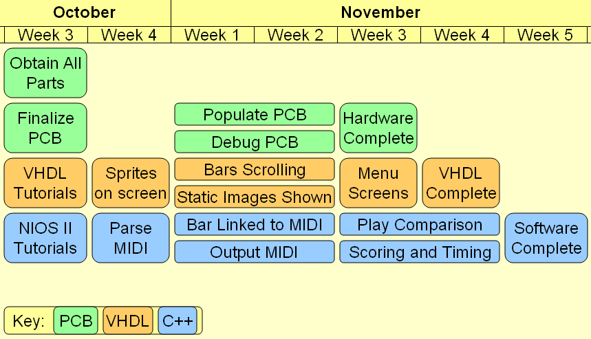
I finished my portion of the design presentation including the power point slides that I will be using during the presentation. I also created a timeline for the completion of our project, which can be seen here:
WEEK 08 SUMMARY
Accomplishments: Finished Design Review Presentation
Weekly Work Total: 6 hours
Project Work Total: 107 hours
October 14, 2007 (2 hours):
We met as a team in the lab to work on a few different aspects of the project. Bryan and I attempted to update our PCB Layout using an updated Schematic netlist, but we ran into a problem of the PCB Layout removing all of our traces and lining up the parts on the peripheral of the board. We are planning on meeting with one of the TA's to find the solution to this problem. I also began researching exactly what our software will have to do in order to interface with the BU8793KN Melody LSI for our audio output. I discovered that the INT pin of the chip needs to be connected to our processor (FPGA pin).
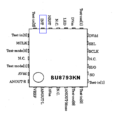
Previously we did not have a very descriptive app note for the BU8793KN so we left that pin unconnected. We will need to update our schematic to fix this problem, but we need to figure out how to update our netlist properly before the PCB will reflect the correction.
October 15, 2007 (2.5 hours):
I sent an email to Phil asking about our schematic and pcb linkage problems, and I am planning on meeting with him during his office hours tomorrow. I read through the Melody LSI application note and began developing an outline of how our software will have to interface with the device. Here is what I developed:
MIDI LSI Start Up Sequence
1. Power On
2. Reset (NRST pin set L at least 10 ms after VDD goes high)
3. Set up the common setup register by writing 0x01 to address 0X00 (see pg 17 of spec)
4. Set total volume settings (write 0XFF to address 0X01 to set MIDI volume to max range)
5. Set FIFO control settings (write 0x44 to address 0x08 for default FIFO full/empty levels)
6. Firmware reset (write 0x80 to address 0x07 sequence control register)
I discovered that the Melody data that is stored in the FIFO (sent by the microprocessor) is formated differently than the standard MIDI format. There are two different types of data with format that can be found on page 23-26 of the BU8793KN spec sheet. The format used by the chip is a MFi format. I searched on google for a SMF(.mid) to MFI(.mld) converter, and I found this website: http://smaf-yamaha.com/tools/nec/tools.html. I was able to download the SSD and SCP converter programs seen below. 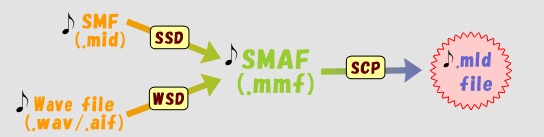
I will experiment with these programs tomorrow and see what a MIDI file looks like after conversion.
October 16, 2007 (3 hours):
I spoke with CHuck about the minimum trace width and spacing. He directed me to the 4pcb.com website to see what the manufacturer's specifications were. WE discovered that the minimum trace width and spacing for our board is 0.006" (6 mils). This is good news because now we won't have to reroute significant portions of our board.
I also worked on synching the schematic with the pcb with Phil's help. After spending a long time trying everything possible, I finally gave up struggling with Orcad, and I started updating the schematic.
October 17, 2007 (2.5 hours):
We had our second design review and after meeting with Chuck we decided to rerout our PCB. We decided to redo the PCB because we couldn't get the schematic synced with our old PCB files, and with all of the changes we were making in the schematic we thought it would be best to have them linked and directly ported to the PCB. I made a few more updates to the schematic, namely I connected the INT pin of the MIDI LSI and I added a few headers to the schematic. Bryan volunteered to do most of the routing for the PCB, and I will be meeting with him tomorrow to help him get the new PCB started.
October 18, 2007 (2.5 hours):
I met with Bryan to start the new PCB. We decided not to change the pin assignments on the FPGA dramatically as we had discussed. We didn't want to make significant changes which would make our old PCB layout irrelevant as a reference for our new PCB layout. I fixed a few of the remaining problems with the PCB, and corrected some errors after running a DRC. I exported the netlist, and got a new PCB up and running. I came back to the lab later to correct some of the PCB footprints that we found problems with. I corrected the following footprints:
MIDI DIN Connector
Audio Jack
DC PWR Jack
MIDI LSI
1000uF Cap
SRAM
It is possible that a few parts remain with incorrect PCB footprints, as I did not check every part with the footprint, I just checked and corrected those that were set aside by Vik and Tom in the box of parts with an "incorrect footprint" label.
October 21, 2007 (3 hour):
I updated the block diagram, and I informed Bryan of the footprints which I had changed. I also realized that the MIDI input voltage is 5V and the FPGA IO pins can only take up to 3.3V; therefore, we are going to need some sort of level translation from 5V to 3.3V. The easiest way to do this at this point may be just to use voltage division across some resistors. Working by myself, I created an overall block diagram for the C++ software that will be run on the NIOSII processor. I then broke down the gameplay block of the diagram to illustrate the logic of that important part of the software. I plan on creating an electronic version of the block diagram, when the logic is more finalized. I will post the diagram on this notebook, when it is finished.
WEEK 09 SUMMARY
Accomplishments: C++ Software Block Diagram and PCB Progress
Weekly Work Total: 15.5 hours
Project Work Total: 122.5
October 22, 2007 (7.5 hours):
I met with Bryan in the morning to finish the PCB. I began looking for a level translator for the MIDI input to the FPGA. I finally found a part that would work, the SN74LVC1T45. I put the part into the schematic and then I realized that we might need to have a pull-up resistor on the DIR pin. I then started questioning whether we had put the proper pull-up/pull-down resistors on our other chips. I added a resistor to the MIDI LSI chip and the oscillator. This then added work to the PCB. I then returned to the lab later and had to fix a few footprints that we discovered had not been updated on the PCB properly. I fixed the footprint for the new level translator and the oscillator. Bryan and I then ran a DRC and found various other PCB errors, which we fixed. We sent the PCB to freedfm.com to see if we had any PCB "showstoppers." We discovered that our PWR and GND vias were too close together and the thermal relief pads were choking some of the connections. We fixed the problems and resubmitted to the website.
October 23, 2007 (1.5 hours):
I discussed the software structure with Tom. I explained the flowchart that I had made and we briefly discussed the pros and and cons of our options.
October 24, 2007 (4.5 hours):
I met with Tom again to make some hardware decisions. These are our two main options for the game display mechanics:
1. Hardware scrolling
Software sends the staging of the bars, basically feeding the bars from the top of the screen. The hardware continuously shifts the play screen downward so that the bars "fall" down the screen. The hardware constantly checks the final pixel row for the presence of a bar for any of the keys. The hardware then tells the software when a bar hits the keyboard icon at the bottom of the screen.
2. Each bar an object
Each bar would be an object with certain attributes. The attributes would be, track, instrument, key, start position, and end position (or alternatively, length and start position). We would have to have a maximum number of bars to prevent the need for dynamic memory allocation.
We decided that a hardware scrolling solution would be simpliar to implement.
Tom and I then began working on getting the NIOSII IDE to function correctly for any of the DE2 demonstrations. We tried using the Linux machines in MSEE190 to run the software, thinking that the software license might work for those machines. We ended up having lots of problems with the linux version not being able to switch workplaces. After talking with Professor Johnson, we were unable to solve the problem so we went back to the 477 lab and retried the windows version of the NIOSII IDE. We were able to download the DE2 VGA MOUSE demonstration and run the Hello World program. There seemed to be a software bug in the actual VGA Mouse program though, as it gave us an error saying that four functions were declared multiple times. We checked extensively and the functions are only declared once in the program. We eventually gave up trying to get that specific demo to work, as we proved the important point that we could program the NIOSII successfully!
October 27, 2007 (2.5 hours):
I successfully wrote a MIDI file to flash using the DE2 control panel software. (You must erase the flash before you can write to it, and the number of writes to flash is limited). I successfully loaded a MIDI file from flash using the same DE2 control panel software. My next goal is to read the MIDI file title and then output the text to the LCD. In working towards this goal I went back to using the DE2 board demos as a starting point. I again attempted to get the DE2_NIOSII_MOUSE_VGA to work using the NIOSII IDE software. I followed the tutorial directions but instead of importing both the hello_world_0 and hello_led_0 projects, I just imported the hello_led_0 project (along with the hello_led_syslib_0). I then clicked "build all" and the program successfully compiled. I ran the program successfully.
WEEK 10 SUMMARY
Accomplishments: Finished PCB and worked out bugs with NIOSII IDE
Weekly Work Total: 16 hours
Project Work Total: 138.5
October 29, 2007 (3 hours):
I built the MIDI input circuit with some degree of difficulty. The MIDI cable provides a current loop as the signal carrier. When the current is on, the signal is asserted. Viewing this operation on the oscilloscope is confusing and misleading. I found this article online, which proved extremly helpful: http://www.circuitcellar.com/library/ccofeature/ball0300/c0300sbpdf.pdf. I hooked up our circuit with the optoisolator recommended in the article (the same one we are using for our design), and the output finally started making some sense. The bit packets sent when keys are pressed can be seen on the oscilloscope. I also realized that we might have a problem with the footprint for our optoisolator. The ones we ordered are through hole, and the footprint is surface mount. We might be able to order surface mount versions of the part. The bit rate of the MIDI stream is 31.25 kbps. We can sample at this rate if we divide our 80MHz clock by 2560.
October 30, 2007 (4 hours):
I found a tutorial online at the Altera website that I could access after registering for an Altera account. The tutorial was an hour long training session that was very helpful for understanding how to use the SOPC builder and the NIOSII IDE. I got through most of the tutorial on the hardware (i.e. SOPC builder and Quartus II) and I began making an overall system on chip that would include the VGA output that Tom had developed and also included a NIOSII processor core with the needed peripherals. Using the SOPC builder, I built a system with the NIOSII processor, Flash interface, LCD interface, and onchip memory. I then had to figure out how to go about combining the generated VHDL code with the code that Tom had developed. Tom and I discussed how this might be accomplished and I did some more research. There is a schematic tool in Quartus II that allows you to link files together using their generated block system file. Tom recommended that we make another VHDL file that would be the top entity and would link the other files. We ended up having to leave before we could link the system.
October 30, 2007 (3 hours):
I found a tutorial online at the Altera website that I could access after registering for an Altera account. The tutorial was an hour long training session that was very helpful for understanding how to use the SOPC builder and the NIOSII IDE. I got through most of the tutorial on the hardware (i.e. SOPC builder and Quartus II) and I began making an overall system on chip that would include the VGA output that Tom had developed and also included a NIOSII processor core with the needed peripherals. Using the SOPC builder, I built a system with the NIOSII processor, Flash interface, LCD interface, and onchip memory. I then had to figure out how to go about combining the generated VHDL code with the code that Tom had developed. Tom and I discussed how this might be accomplished and I did some more research. There is a schematic tool in Quartus II that allows you to link files together using their generated block system file. Tom recommended that we make another VHDL file that would be the top entity and would link the other files. We ended up having to leave before we could link the system.
October 31, 2007 (2 hours):
I soldered our level translator to a surface mount proto board so that we could reduce the 5V signal coming from the MIDI keyboard to the 3.3V that will go into our FPGA. I then worked with Tom to continue our efforts to link the VHDL files in our system. I finally found a useful page in the Quartus II help menu that showed us how to build an overall schematic for our system and to link the generated block diagrams for our two VHDL files. We successfully linked the files and were able to put the .sof onto our dev board. I then began looking at programming the processor with the NIOSII IDE. I made some progress but then realized that I forgot to add on-chip memory to our system. I added the memory but then was confronted with an error that said that the global pointer could not reach the location of the memory due to the limited values of the pointer offset.
November 1, 2007 (3 hours):
I returned to the error I was receiving yesterday with the pointer offset. I moved all of the memory components of our system to the begining of the FPGA memory, and I also had to grow the size of the onchip memory significantly. The very simple Hello World program that I was loading onto the FPGA was 56kbytes, so I made the memory larger so that it could hold the program. I then started getting this error again:
Using cable "USB-Blaster [USB-0]", device 1, instance 0x00
Pausing target processor: not responding.
Resetting and trying again: FAILED
Leaving target processor paused
I did some more searching online and I discovered the cause of the problem. When the .sof file is loaded onto the FPGA using the QuartusII programmer, a dialog pops up saying "Click Cancel to stop using OpenCore Plus IP. Time Remaining: unlimited." If you click cancel and attempt to run a program on the NIOSII you will get the above error, but if you leave that dialog window open, the program will run on the board. After I did this, a new error surfaced and I realized that I did not have the correct .sof loaded for the program that I was trying to build. I had made some changes to the SOPC but I had not recompiled the project in QuartusII. I realized this mistake and I recompiled the project and discovered that I had assigned too much onchip memory, and I was using 226% of the available memory. I backed that memory down significantly and recompiled the program. I will need to set that memory down to the amount available to us on our smaller FPGA eventually. At this time it is still too big, but until I figure out how to load the program onto flash instead of on-chip memory, I need to keep the memory size large. I figured out how to load the program onto flash memory, but then I realized that I had made a few other errors loading the correct .sof file onto the board so I will need to fix those tomorrow.
November 2, 2007 (7 hours):
I attempted to load a simple Hello World program onto the system that I developed with the SOPC builder combined with the VHDL that Tom had developed. I ran into many problems with very non-descriptive error messages.
November 3, 2007 (10 hours):
I found a simple tutorial to try for a NIOSII system. I was very frustrated with my lack of progress yesterday, and so I developed a simple list of tasks to perform to get to the bottom of our problem. I found a simple tutorial, and I followed it exactly, but again I arrived at the same pausing processor: not responding error message. I gave up on that tutorial, and somewhat out of desperation I went back to a demonstration that I knew worked and I compiled it and loaded it, and it ran fine. I then attempted once again to build a system with the SOPC builder that would use Tom's VHDL file. I attempted to build a custom component using Tom's VHDL file (with our gameplay and VGA output hardware design), but that proved unfruitful. I then linked went through yet another tutorial online from the Altera video demonstrations site, and although the system built in the tutorial wouldn't fit on our board, some slight modifications made it fit. I linked Tom's VHDL file and finally the NIOSII processor was able to load and run a simple Hello World c program. I still haven't the faintest idea what has been causing our problems. It seems that some slight variation in the system constructed with the SOPC builder causes the error. I've moved on from that error, now that I have something that works. I made a few important discoveries while going through this painful process. First I realized that you can import pin assignments from the DE2 CD, which saves a lot of time. I also discovered that the EPCS config device only stores the program and .sof files, but when the program is run it must be putn into onchip memory or into another form of volitale memory. Since I now have a system that works for the most part, I started attempting to use a template C program to load a MIDI file. I used the template "host_filesystem". One thing that concerns me with this template is that you must use "Debug As -> NIOSII Hardware" in order for it to work. The reason being that the Host File System feature relies on a GDB server running, which only occurs in the "Debug As" mode.
I attempted to run this C project on the system that includes Tom's VHDL files, but I ran into problems because the on-chip memory in the system was not big enough to hold the program. I then tried to enhance our system with the SDRAM available to us on the DE2 board. First of all I realized that we can't clock our SDRAM at 80MHz, because the longest latency is 12ns for the write cycle time, which is about 83.33 MHz. I suspected that this might be the case while looking at one of the demonstration designs that used SDRAM and had a sys_clock of 100MHz and yet only a 50MHz clock for the SDRAM. I chose to put the SDRAM clock at 40MHz. I added the component, generated the system, compiled the hardware, programmed the hardware, built the C project, and then ran the program as Debug, and I got a validation error. I researched this error and found that it is common for SDRAM components. This forum proved quite helpful: http://forum.niosforum.com/forum/lofiversion/index.php/t3192.html. From reading these forums I realized that there has to be a phase shift in the SDRAM clock from the system clock. I shifted the (40MHz) SDRAM clock by -3ns from the (80MHz) sys_clock, but I got the same problem. Then I tried (40MHz -3ns) SDRAM clock and (40MHz) sys_clock, same validation error. Then I tried (40MHz -3.5ns) SDRAM clock and (40MHz) sys_clock, because I saw some had tried that with success on the forum. That also failed. I think I am going to have to delegate either system operation or writing C code to someone else on the team, because we need to progress in both of those areas right now, and it's too large of a task for me to do both at the same time. I haven't done any C code development yet. (I also installed QuartusII and NIOSII IDE on our notebook (pc4) so that Tom and I can both develop and test hardware at the same time).
WEEK 11 SUMMARY
Accomplishments: I began learning a significant amount about how to use the SOPC builder and the NIOSII processor. I encountered many problems, that I still need to work out, but I did make some progress in taking the tutorials.
Weekly Work Total: 32 hours
Project Work Total: 170.5 hours
November 5, 2007 (9 hours):
I researched what we could use for a very basic file system to use for storing and opening MIDI files. I found a very good template program for such a file system on the NIOSII IDE new project menu. I did some reading about the HAL (hardware abstraction layer) system and about the file system that can be used with the processor and a flash device. This pdf had lots of information on the zip file system: http://www.altera.com/literature/hb/nios2/n2sw_nii52012.pdf. I read through this documentation and then attempted to compile the program. I discovered that the program would not fit in our on-chip memory so I had to add an SRAM component to our SOPC system. I realized that on Saturday (11/3) I had added an SDRAM component, which our final design does not include. I removed that component and added the SRAM. I had to copy the component used in the DE2 board demonstration folder in order to get the correct SRAM component. After I generated the system with SOPC builder, I linked the schematic symbols, added the pins to the pin planner, compiled the system, programmed the FPGA, built the C project, and attempted to program flash as the project recommended. I ran into some problems with the EPCS device. The flash programmer kept giving me the following error:
Using cable "USB-Blaster [USB-0]", device 1, instance 0x00
Resetting and pausing target processor: OK
Reading System ID at address 0x00112028: verified
No EPCS layout data - looking for section [EPCS-FF]
Unable to use EPCS device
Leaving target processor paused
I submitted a mysupport ticket at the Altera website, and hopefully I will hear back from them tomorrow. I decided to switch gears and work on sending data over to the hardware. I added PIO to the SOPC builder, and also a timer module. I then made a very basic C program to output to some PIO registers, which I connected in the schematic to some ports that Tom created in his VHDL file. We ran into some problems with Tom's file using too many logic elements. He's going to talk to Dr. Johnson tomorrow. I will test the C program tomorrow. I built it twice and I had some errors that I will need to work through.
November 6, 2007 (8 hours):
I discovered that the read-only zip filesystem template in the NIOSII IDE only works for CFI flash devices and not for the EPCS. I began researching how I could use the EPCS as a file system or at least be able to store a file to the device and then load it into SRAM. I realized that I was recieving an error when I attempted to use the flash programmer to load a single file onto the EPCS device. I filed a mysupport ticket with Altera for help with the problem. I also wrote a simple program that could send data to Tom's VHDL to control which bars would descend from the top of the screen. I ran into a few problems, but eventually I just recreated the NIOS II IDE project and after reexamining my code, I discoverd a simple syntax error that was causing my problem. The software successfully communicated with the hardware, and the bars could be controlled. The remaining time I spent on the project was the safety and reliability considerations needed for the next homework. I made a presentation for the TSCP session tomorrow.
November 7, 2007 (6 hours):
I heard back from the Altera my support ticket that I filed yesterday, and I discovered that there was a simple cause to the flash programming problem. The run/prog switch must be in the run mode when using the flash programmer (this is a little counter intuitive, which is why I made the mistake for so long). I was able to successfully load a MIDI file into the EPCS flash memory. I met with Tom in the lab, and while he worked on the VHDL code for the MIDI input, I worked on reading from flash memory. I decided to use the simple flash API functions that are generated by the hardware abstraction layer creation, instead of trying to create a file system on the EPCS device. I wrote a program that could load data from flash. I ran into many problems with the data format as it is read. I eventually figured out that I had to read the data from flash into an array of unsigned chars in order to properly store the memory in a format that was usable. I also realized that the "read from flash" function uses a length parameter that signifies the number of bytes to be read. I had initially thought that this length value corresponded to the bits being read, so I had to correct a few mistakes in my code. By the end of the day I was able to read the file header and determine the file format, number of tracks, and the delta ticks per quarter note for our sample Bubble Bobble midi file.
November 8, 2007 (4.5 hours):
Working alone, I continued where I left off with the programming for parsing through the MIDI file. I made significant progress in parsing through the midi file. Some of the big things that I learned was that I will have to be careful about facilitating the variable length time bytes that MIDI is fond of using. I had made some assumptions about the time bytes (only using 1 for instance) that proved to fall through in the end. I corrected those assumptions and fixed the code so that it was roboust enough to parse through our bubble bobble MIDI file. At the end of the day in the lab, the program can parse through a MIDI file, output the song title, the composer, the track names, and also output the notes that are being played. The next step will be to device a mechanism of sending the note data to the hardware with the correct timing. This is going to be tricky because MIDI uses numerous channels that can be played simultaneously. The MIDI file that I have been working with utilizes two channels playing at the same time. It might be better to do the simultaneous computations in hardware, but I will need to check with Tom about that first.
WEEK 12 SUMMARY
Accomplishments: Significant progress was made in parsing through MIDI file. I was able to load a file from flash, parse through a track, and extract all of the relevant timing and note information from the track.
Weekly Work Total: 27.5 hours
Project Work Total: 198 hours
November 11, 2007 (5 hours):
I met with Tom in the lab to work on the MIDI song parsing and the output to the VGA monitor. While Tom worked on the MIDI input VHDL, I developed the C software to read through the MIDI file and then output the notes to the hardware at the proper time. I created a function that would play the notes contained in a note array. The function steps through the array and asserts the proper note bit for the amount of delay specified for each note. By the end of the day the software was reading through the Bubble Bobble MIDI file and outputing the notes to be played to the hardware with the proper timing. The only downside is that the two channels are being played one after another and are not playing simultaneously. I had thought that this might be easier in hardware, but I think I can do it in software with some clever sorting of the notes array.
November 12, 2007 (9 hours):
I met with Bryan and Tom in the lab to continue work on the software. I had the goal of outputing both channels simultaneously. I developed a function that inserts notes into the Notes Array in the proper order given the timing of the different channels. After struggling for a good amount of time with this function, I took a break and when I came back I was able to solve the problem in a few minutes. At the end of the day I was able to output both channels of the Bubble Bobble MIDI to the screen with the correct timing and notes. After this success I switched gears to tackle the audio output. I soldered the MIDI LSI chip to a protoboard and added headers to the board to facilitate testing with the DE2 board. I then modified our FPGA system using SOPC builder to add an additional PLL output, a SPI interface, and some extra PIO for the additional inputs and outputs to the MIDI LSI chip. While working on this task, Bryan and Vik were having trouble with the 1.2 V plane on our board. Bryan had just put the FPGA on our PCB and afterwards he tested the 1.2 V power and ground isolation and found that there was only 50-60 ohms between the 1.2V plane and ground. Bryan had tested the power before adding the FPGA and found that it was fine. We closely examined the FPGA pins and the various other parts. After many hours of testing we decided to wait to talk to Chuck tomorrow to see if he has any ideas for us.
November 13, 2007 (6 hours):
I met with Tom, Vik, and Bryan in the lab. I began developing a pseudo-code flowchart for the audio output via the MIDI LSI. The MIDI LSI is a very complex chip that functions as a small microprocessor essentially. There are many control registers that must be set during the initialization, and the data must be sent in a proper format. In making the pseudo-code I noticed a few problems with the SOPC builder configuration I had made yesterday, and I made the necessary changes. I began testing the initialization of the MIDI LSI and playing simple songs. I developed a function that will initialize the MIDI LSI, but in order to do that I first had to test the SPI. I tested the SPI block which I added in the SOPC builder, but it didn't seem to be giving any out put when assigned to an I/O pin on the FPGA. I'll have to get that working tomorrow.
November 14, 2007 (6 hours):
I met with Tom, Vik, and Bryan in the lab. I continued work on the SPI block, and I managed to get the SPI working alright. I developed some more code to send data to the MIDI LSI. I had to solder some connections to our MIDI LSI chip in order to be able to test the board. I connected many of the required pins, but I was unable to test the software due to SPI problems. I discovered that the SPI needed to be changed to facilitate 16 bit data transfer instead of only 8 bit.
November 15, 2007 (6 hours):
I met with Tom, Vik, and Bryan in the lab. I helped Vik solder the MIDI LSI chip onto our PCB. It was really difficult to solder the chip because the package was unusual. The chip has a lead-less package that was very difficult to get lined up and soldered. After spending quite some time working on the chip (desoldering the chip entirely once), we finally got it on the board. I did a little more work on the MIDI output code so that we could test playing a song. I will still need to change where the MIDI file is stored and how it is referenced due to the transition from the DE2 board to our actual PCB. I have been running our C code from SRAM instead of loading onto the EPCS flash device. With our actual PCB we will need to load the code into the flash device and we will need to store the MIDI file in a place that will not get overwritten by this code. We tested our PCB by loading our Quartus II project onto the board successfully. Next step is to load the C code.
November 16, 2007 (3 hours):
I attempted to load the C code, but I ran into multiple problems. I was unable build the C project because it would not fit onto the specified memory location. I realized that this was the case because the memory location specified for the program in the system library properities was the on-chip memory, which isn't very big. I tried to switch that memory location to the SRAM, but I then I discovered that the memory was not showing up in the list of available memory devices. I began investigating how to write a driver for the memory component. There were many documents to read about this topic, and the task grew in complexity. I decided it might be better to try to modify the existing sram component driver for the sram on the DE2 board. I tried to find this file without any success. I'm not sure where it is or if it is the device driver that actually specifies the memory as available for the linker script. I ended up leaving frustrated and hoping that tomorrow I will be able to attack the problem with some fresh ideas.
November 17, 2007 (5 hours):
I came into the lab by myself and started thinking of some ways to solve our sram problem. We had thought about just purchasing the sram used on the DE2 board, but I didn't want to have to wait for that chip to come in to progress on our actual board. I decided to try modifying the existing sram component for the DE2 board by changing the VHDL file in the folder but leaving the perl script and other files the same. I rebuilt the system and compiled the Quartus II project and it was successful. Now our sram can be chosen for the program location in the NIOS II IDE program. (The name of the sram component is the same as the DE2 part, which is misleading, but I didn't want to change the file and screw up any file associations in the other files in the component folder. The sram is named sram_16bit_512k, when it should be named sram_8bit_512k. Nothing too major, but something to be aware of.) With this problem solved, I again attempted to program the Cyclone II FPGA on our board with the flash programmer tool in the NIOS II IDE. I received an error stating that no JTAG device is found. I looked into the requirements for a JTAG device and I found that our system has all of the needed components. I went to the altera website and I found this table and description which could explain our problems: 
But this table shows that the JTAG configuration mode takes precedence over the other configuration modes. I then found another table in the FPGA datasheet in the configuration chapter: 
Our PCB has TDO as a no connect, TMS wired high, TCK to ground, and TDI wired high. We'll need all of these pins in order to program with JTAG. Bryan is going to talk to Chuck Monday about flywiring all of those changes. In the meantime I reassigned our pins on our old project to continue development on the DE2 board. I hope to test the MIDI (audio) output tomorrow and get that all working.
WEEK 13 SUMMARY
Accomplishments: We finished soldering the MIDI LSI chip to the board. I began investigating the use of the SPI peripheral. I ran into many problems with the SPI and using JTAG. I discovered that we will not be able to program our board using JTAG.
Weekly Work Total: 40 hours
Project Work Total: 238 hours
November 18, 2007 (5 hours):
Now that we have discovered problems with programming our own PCB, I reverted back to using the DE2 board to test the audio output. I had previously mounted the MIDI LSI chip (a tiny cell phone chip) onto a surface mount protoboard, but the MIDI output circuit had to be wired on this protoboard. Vik helped do this by soldering wires across the protoboard to create the circuit in our schematic for the audio output block. While Vik was preparing the chip, I began investigating the SPI more thouroughly. The MIDI LSI chip communicates with a host processor through an SPI interface, which I discussed a little bit earlier. I had thought that the SPI was working fine, but I discovered that I was sending extra packets of garbage data after each desired send. I discovered this using the debug tool in the NIOSII IDE. I was able to modify the spi_send functions easily to solve this problem. I then created another function called spi_read, which would send an address on the LSI and read from that address over the SPI. Tomorrow I will continue work with the SPI and begin actually testing with the LSI chip.
November 19, 2007 (10 hours):
I continued work on the SPI output. The SPI was operating inconsistantly and the program was freezing at times. There are very few places where the program could enter an infinite loop, therefore I thought that it would be easy to locate the problem. The trouble was that the problem does not occur when the debugger is used. While debugging the spi_send and spi_read functions I discovered a rather bizarre error in which the pointer pointing to the read_data would not dereference properly. I could not change the value stored at the memory location pointed to by the pointer. I ended up rethinking both our spi_send and spi_read functions, and I trimmed them down to just what was necessary removing pointers entirely just for good measure. The SPI was then functioning adequately with no connection to the MIDI LSI chip. I then added the LSI chip, and the communication wasn't working. After testing quite a few different theories, I discovered that I had a typo in my code that caused the MCLK (the system clock of the MIDI LSI) to be turned off. After I corrected that error, the first 20 notes of the MIDI file loaded in the program began playing over the speakers. There was much rejoicing. Bryan and I began developing the logic for the audio output. The MIDI LSI has a FIFO buffer that can hold about 20 notes at a time, therefore throughout the playing of the song we need to fill the FIFO buffer with notes. The trouble is that the audio output must be occuring at the same time that the software is managing the display of falling bars. This display function enters into a usleep function (a wait loop) when it does not need to toggle a bar on or off. We discussed the possibility of maintaining a count of the notes in the buffer and then adding notes to the FIFO during this waiting period between bar toggling. We will further address this problem tomorrow. Chuck also finished modifying our board to allow JTAG programming. We will test this tomorrow as well.
November 20, 2007 (10 hours):
Meeting as a team, I continued working with Bryan to develop an effective way to output the audio while managing the display of the falling bars. We performed a few tests to see how long the spi_send function lasts, and we determined that the overhead of sending notes to the FIFO is too significant to be ignored (163.6 us per note, which accumulates). We decided that we really only had two options, either we could take a multi-threaded approach and attempt to load a real time operating system (RTOS) on the microprocessor, or we can modify our usleep wait function to load songs into the FIFO while our display function is sleeping. The NIOS II IDE provides software templates for the RTOS that seem fairly straight forward, but Bryan came up with an easier method of modifying our wait loop. Vik found a function using the timer peripheral that provides an easy way to measure the clock cycles between the execution of different sections of code. Instead of using the usleep function we now enter into a loop that uses this timestamp function to check the time. If there is sufficient time, and the FIFO is nearly empty, then we add notes to the FIFO until it is either nearly full or we are out of time. When we are out of time we enter into a tight wait loop that uses up any extra time we might have, and then the display function continues. In this way, the timing of the bars output to the screen is maintained and we can service the audio output. Some problems still remain however, as the bars do not line up perfectly with the audio output, and the error appears to accumulate.
I also tested a new MIDI file instead of the Bubble Bobble theme song that we've been testing up to this point. Luckily the new song (the Tetris theme A) worked great except for one small problem with the audio. When we load the audio into the FIFO, the data format allows only one byte for the time stamp of the note event. The MIDI standard uses a variable length for the time stamp, and it can be up to 4 bytes long. I knew that this might be a problem, as my code would just truncate the time stamp to one byte. With Vik and Bryan's help, I made a few slight modifications to the code, so that a nop (no operation) of the extra time would be added to the FIFO to account for the excess time discarded in the one byte time stamp of the FIFO note format. The audio is still not synced with the bars, and I will need to rethink our logic to some degree in order to get better synchronization. Adjusting timing will help us to some degree, but errors will still accumulate. Aside from this progress with the audio output, we also tested the JTAG. It failed. We performed many tests to try to determine the source of the problem. we checked the cable and it seemed to be working fine. We check and double checked, and triple checked our circuit, and it looks great. We scoped the signals from the JTAG cable onto the board, and it appears that our FPGA is even responding to the JTAG signals (the TDO pin shows a signal, and we assume that it is data out), but the software cannot detect the device. I ended up submitting a ticket with Altera asking if there was a way to load our software onto the FPGA without using JTAG, and by the end of the day they had responded with a pdf titled solution1. I wish they could send us more of those). The pdf explains how to use active serial programming to load software and other files onto the board. I will test it tomorrow.
November 21, 2007 (5 hours):
Working on my own, I came to the lab and tested the programming method detailed in the solution1.pdf. I transfered the C program from the DE2 board project to our PCB project. I had to comment out all of the printf statements because we do not have JTAG supported on our board. I followed the following steps to program our board:
1. convert sof file to .flash using sof2flash command in the NIOSII command prompt.
2. convert the .elf programming file to .flash using elf2flash, indicating that it will be placed in memory after the .sof.
3. Generate .pof from only the .sof file using the QuartusII programmer. Open the memory map file that is generated (.map file).
4. Record the end address of the .sof file in memory: (0x00076C9F for this test).
5. Convert the software from .flash to a hex data file using the provided flash-to-absolute-hex script (use the end address from step4 as the second argument in the command after the filename.
6. Generate new memory map.
7. Convert the MIDI file to absolute hex at address 0x014FFFF (far away from the configuration file and the program data).
8. Generate .pof after loading all files.
I successfully downloaded everything but the program is not running. Maybe a problem with the reset vector? I discovered that I was placing the first byte of the software onto the last byte of the configuration file, but even after fixing this problem, the program still would not load. After Thanskgiving, I will tackle this problem.
WEEK 14 SUMMARY
Accomplishments: Got MIDI LSI to work using the SPI! We now have audio output working on the development board, which is a huge accomplishment considering the complexity of the MIDI LSI chip. We also found an alternative method of programming our board aside from using JTAG.
Weekly Work Total: 30 hours
Project Work Total: 268 hours
November 26, 2007 (6.5 hours):
I came to the lab to work on my own to see if I could get the program to load successfully. There were two main tasks that I hoped to accomplish today:
1. Get the boot-up sequence to work properly with the software as I had attempted before break.
2. Sync the audio better with the falling bars on screen.
In attempting to solve our first problem, I tried switching the reset vector for the microprocessor to SRAM, but that did not solve our problem. After frustrating many other options for fixing the software boot-up problem, I switched gears to address the audio problem. I thought that the best way to sync the audio would be to have Tom write the hardware to tell the software which bar is hiting which key, and then the software could output the correct note at the exact time. I toyed with a few different ideas as to how to implement this method, but due to limited playback control on the MIDI LSI, that method was going to prove to be very difficult. Instead I examined the timing of the MIDI LSI output. I discovered that the actual MIDI LSI frequency is 16.6666 MHz / 130 = 128.205 kHz. The desired frequency is 128 kHz exactly. This small descrepency would only account for an accumulation of 192 msecs of audio mismatch after 2 minutes of playback, which isn't extremely significant. I then realized that our actual PCB will be using a different clock, which can easily acheive the 128kHz exact clock using a PLL. With the help of Vik and Bryan we discovered that the audio portion of our code had a few logic errors. The midi standard has variable length byte(s) that correspond to the time delay before each midi event. The MIDI LSI only has one byte for time delay. No-operation (nop) events have to be added to the MIDI LSI FIFO buffer before notes that have longer than one byte of time delay. Previously our code did was only adding one nop event for each extra byte of time delay. This was incorrect because the nop event only provides 0xFF delta time ticks of delay. We had to rewrite this section of code, and the audio synchronization was vastly improved.
November 27, 2007 (4 hours):
I worked on getting the software to load on our PCB. I submitted another altera help ticket on our mysupport page to see if they could help us. I attempted to replicate the commands issued by the NIOS II IDE flash programmer using the NIOS II command prompt. This method failed however, as using the flash programmer commands apparently requires the use of a JTAG device. I gave up this method and continued to investigate the problem.
November 28, 2007 (4.5 hours):
I investigated the hex files and flash files. I thought that I might have found the answer to our problems when I discovered that the addresses were different for a hex file and for the flash file that the flash programmer uses to (successfully) program the DE2 board. I then discovered that the reason that the addresses were different is because I was not compressing the .sof file when I generated the .pof. I compressed the .sof and tried again, but the progam still wouldn't load. Finally Vik found that someone had experienced the same problem on an Altera forum, and they solved it by just unplugging the USB byte blaster cable from the board. We did this and the program ran successfully.
November 29, 2007 (2.5 hours):
Working with Vik. After running our C code on our board we noticed that the audio output was not functioning. We began debugging that segment of the circuit. Vik searched through out PCB and schematic documentation and realized that we had our pins mixed up for our audio jack. I desoldered the jack and then we hot glued the jack upside down over its original place so that we would have access to the pins to fly-wire them correctly. Bryan finished fly-wiring the audio jack. We retested the audio and it failed again.
WEEK 15 SUMMARY
Accomplishments: We successfully programmed our own PCB using active serial programming! This is an extremely important step, because without this ability we would have to change something drastically to be able to program with some other method. We also discovered a few more errors on our PCB that we will need to fix.
Weekly Work Total: 17.5 hours
Project Work Total: 285.5 hours
December 2, 2007 (6.5 hours):
I worked with the rest of the team. I discovered all sorts of new problems that we weren't experiencing before. We ran out of disk space on our team network drive, so I transfered everything to our hard drive. I also soldered the header for J12 where we were also outputting the MIDI LSI SPI signals. When I compiled and ran the program from the new location, we got some very unexpected behavior. The program would run for a little bit and then it would just terminate. The time of termination varied among different trials. We noticed that we were receiving some timing warnings after compiling our project due to the processor using an 80Mhz clock, while the other hardware components used only a 40MHz clock. We changed all of the clocks to 40MHz and Tom integrated his hardware development into the project for our PCB. After recompiling this system the video output became horribly distorted. Not good.
December 3, 2007 (8.5 hours):
we met as a time to tackle our newfound video output problem. I considered everything that had been changed since the last time that our video output worked correctly. I sought to undue much of what we had done, so that we could settle back into a working hardware setup. I thought that perhaps the header on J12 could have some pins that are shorted somehow. I removed this header and I removed the SPI from the SOPC system, and then recompiled the system. When I loaded this configuration, the video output distortion problem was fixed. We then sought to fix our audio output problems once again. I took a close look at the DE2 board schematic and noticed that there were 47ohm resister packs in series with the IO pins leading to the FPGA. We added these resistors, re-enabled the SPI component in our system, and tested the audio output. The resistors did not solve our problem, but the SPI signals did seem to be less noisy. Bryan and Vik had the idea to capture the output of our PCB SPI output and then compare it to the SPI signals on the DE2 board. After making this comparison, we realized that the SCLK frequency of the SPI on our pcb was only 10MHz not the 13.33MHz on the DE2 board. This was due to our fixing the timing issues by putting everything on the 40MHz clock, including the SPI component. We changed the clock back to 13.33MHz, ran the program, and the audio output began working on our board (using the protoboard mounted MIDI LSI chip via the J12 header). Some logic errors remain with the audio however, as the audio of the last few notes of the song don't match up correctly. All of our PSSCs can now be performed. We will perform them tomorrow before we make any changes that could endanger our system.
December 4, 2007 (13 hours):
We met as a team in the lab to continue fixing the remaining problems that we are having. Our current project can perform all of our PSSCs, which we demonstrated to Phil and Karl. We attempted to load a midi file for a Five For Fighting song, but it failed. I debugged the code on the DE2 board to determine the cause of the problem. I was reading in the track number and quarter notes per delta time data wrong. I fixed this problem and successfully loaded the MIDI file. I was going to fix the problem of the audio mismatch late in the songs that we play, but Vik began work on developing a more permanent fixture for our MIDI LSI for the board. We determined that the MIDI LSI chip on our board won't work, because we need 47 ohm resistors from all of the signal pins. Instead, we are going to use MIDI chip on a small daughter board which will plug into a header on our PCB.
December 5, 2007 (3 hours):
Fixed problems with MIDI parsing. Problem with channel numbers. Made assumptions that only worked for specific MIDI files. Still have some problem with 100years MIDI.
December 6, 2007 (21 hours):
Working with the rest of the team in the lab, I fixed a few problems with the software. We were not accounting for time delays for all MIDI events, which can screw up the timing for certain MIDI files. I also discovered another problem where our time stamp variable was being overrun. I was able to get the software working pretty well for carol of the bells and tetris, but we are still having a few problems with some of the longer songs with many tracks. After fixing up the software to a point that would work for demonstrations, Tom and I went to wal-mart to purchase some spray paint for the enclosure. We finished the packaging, drilling holes for the various ports, and painting the enclosure. After we finished the packaging we went to Hillenbrand (where Bryan is an RA) and we filmed our video. After we filmed the video we began the lengthy processes of editing the video. We ended up staying up all night in order to finish the video. We then presented our project to ECE270 and ECE362.
December 9, 2007 (7.5 hours):
Fixed audio glitch at end of song by adjusting a variable that did not reflect our updated clock frequency. Fixed the audio glitch at the end of carol of the bells that resulted from not being able to fill up the FIFO buffer quick enough to continue song play. I attempted a few other methods of solving the gradual audio offset that accumulates for the longer songs, but nothing seemed to work. I might try to hammer that out later. We spent the rest of the night finishing up our final project and senior report.
WEEK 16 SUMMARY
Accomplishments: We successfully demonstrated all of our PSSCs! We created a video highlighting the functionality of our project in a creative way, and we demonstrated our project to ECE362 and ECE270.
Weekly Work Total: 59.5 hours
Project Work Total: 345 hours