Article

Characterization of Raman Spectroscopy System Transfer Functions in Intensity, Wavelength, and Time

Lyles School of Civil Engineering, Purdue University, West Lafayette, IN 47907, USA
*
Author to whom correspondence should be addressed.
Instruments 2020, 4(3), 22; https://doi.org/10.3390/instruments4030022
Submission received: 30 June 2020 / Revised: 28 July 2020 / Accepted: 29 July 2020 / Published: 5 August 2020
(This article belongs to the Special Issue Photonic Devices Instrumentation and Applications)

Abstract

:
The emergence of a wide variety of relatively low-cost compact spectrometers has led to an increase in the use of spectroscopic techniques by researchers in a broad array of fields beyond those that have traditionally employed these analytical methods. While the fundamental elements and functions of Raman systems are generally consistent, the specific components that compose a system may vary in number, design, and configuration, and researchers often modify off-the-shelf spectrometers for unique applications. Understanding the effect of instrument design and components on acquired information is thus crucial and provides the prospect to optimize the system to individual needs and to properly compare results obtained with different systems while also reducing the potential for unintended misinterpretation of data. This paper provides a practical treatment of the influences in a typical compact spectroscopy system that can impact the extent to which the output of the system is representative of the observed environment, a relationship that in measurement science is classically termed the system transfer function. For clarity, the transfer function is developed in terms of traditional Raman output parameters, namely intensity, wavelength, and time.

1. Introduction

Raman spectroscopy is named after physicist C.V. Raman, who discovered the instantaneous inelastic light scattering phenomenon in 1928 [1]. The technique provides rich information to identify and characterize materials and has gained popularity because of both its simplicity and diverse range of applications. In this method, a monochromatic light source, usually a laser, is directed toward the target sample. Interaction between the incident photons and molecules of the sample scatter the incident light. While the majority of these scattered photons leave the sample at the same frequency at which they arrived (referred to as elastic or Rayleigh scattering), a small fraction of the photons may exchange energy with the molecules, leading to inelastic, or Raman scattering. In this latter case, individual incident photons may either lose energy (Stokes-shift; most common) or gain energy (anti-stokes-shift). For any given scattered photon, the amount of energy transferred is indicative of a vibrational and/or rotational energy state of the target molecule bonds and thus offers insight into the composition of the sample. To obtain this information, scattered photons are collected and guided to an instrument that separates spectral constituents. A light-sensitive detector is then used to assess the intensity of the scattered returns as a function of frequency to develop a Raman spectrum that reflects the molecular composition and structure of the sample.
The rapid advance of Raman spectroscopy has been driven significantly by innovation in the underlying technologies that compose Raman systems. Developments in semiconductors have fostered the advent of compact, low-cost lasers across a wide range of operating frequencies. Advances in optics production, optical coatings, and fiber optics have enabled greater flexibility and customization in system designs. Developments in light detection and data acquisition have improved Raman system sensitivity and speed. Collectively, these advances have helped make the Raman spectroscopic technique more prevalent in both laboratory and field settings, with particularly strong growth in the use of compact Raman spectroscopy systems and even portable instruments for chemical analysis in applications such as food security [2,3], art examination [4,5,6], in situ mineral detection [7], explosive detection [8], product quality control [9], forensic science [10], and environmental monitoring [11,12].
Due to the broad array of applications for which Raman spectroscopy is employed, Raman spectroscopic instruments may encompass a variety of context-specific components. It is essential to know how each of these components contributes to variations in the properties of the optical and electrical signals propagated in the system and to evaluate and understand the possible output of the system before interpreting results derived from its use. One should also understand the significance of these possible variations before comparing the results of different researchers. With these perspectives in mind, this paper develops the generalized transfer function of a Raman spectroscopic system for the parameters of intensity, wavelength, and time and then applies the generalized formulation to a specific Raman spectroscopic system as an example.
This paper first introduces several general components in a Raman system and provides an overview of how the Raman phenomenon is induced and observed in a typical system. Transfer functions for output characterizing quantities of intensity, wavelength, and time are then developed by following the sequence of light propagation through a system, from the laser source to the sample, and to the detector and data acquisition electronics. For the intensity analysis, energy losses when light propagates through different components in the system are of greatest concern. The wavelength analysis highlights changes in the wavelengths managed and/or observed as light traverses the system. Lastly, the time delay analysis draws attention to group delay and signal spreading which may occur in fiber optic and electronic components, respectively.

2. The Components in a Raman System

A Raman spectroscopy system requires a coherent optical source (usually a laser), a device to selectively examine bands of optical wavelengths composing the scattered return, and a detector to assess the scattering. In a typical lab benchtop Raman spectroscopic system, there are also usually optics to collect, direct, and focus the light; to eliminate unwanted frequencies; or to divert part of the light (for example as a trigger for data acquisition). There is also usually a sample holder that contains the sample of interest (often a cuvette). In a portable Raman system, the device may directly focus on the environment of interest without a container to hold the target. No matter what kind of Raman spectroscopic system, all components along the inbound and return light paths as well as all connections and conduits between the detector and the data acquisition unit influence final observations. Figure 1 shows a schematic of a simple Raman system, and Table 1 lists common component selections.
With an overview of the components of a typical Raman system, it is now possible to examine the overall system transfer function—that is the mathematical expression which theoretically demonstrates the Raman system’s output for each of the possible influences on the input. This will be explored in the following sections by examining component-by-component influences on system output intensity, wavelength, and time characteristics. This discussion follows the sequence of a typical light path in a Raman spectroscopic system, from the excitation source to the sample on to the dispersive device, to the detector, and to data acquisition system, examining optical and electronic components and highlighting related influences on the studied variables at each stage.

3. Transfer Function: Intensity

The transfer function discussion begins here by examining the influence of Raman system components on optical intensity and related electronic signal outputs.

3.1. From the Excitation Source to the Sample

3.1.1. Laser

For a laser of wavelength, λ laser (nm) the output can take two forms. It may either be continuous wave (CW) or pulsed (P). If the laser is CW, the average power can be denoted by, P CW (W). Further, the intensity, I Source = I CW (W/cm2), of the laser can be defined as a function of its beam diameter, which, under the assumption of a Gaussian beam profile, is typically deemed the diameter of a circle containing 1 / e 2   of the power, where e is Euler’s number.
The energy, E CW (J), emitted by the laser over a given time, ton (s), is thus defined as
E CW = P CW × t on
For a pulsed laser, the laser is usually characterized by its pulse width, t pulse (s); repetition rate, γ laser (Hz); and average pulse energy, E pulse (J), The average power of the pulsed laser can thus be denoted by
P P = E pulse × γ laser   ( W )
and its intensity, I Source = I P , again in (W/cm2).
Thus, the energy, E P (J), emitted by the laser over a given time, t on (s), is defined as
E p = P P × t on = ( E pulse × γ laser ) × t on
A parameter, E Source , representing either the E CW for a CW system or E P for a pulsed system, is introduced here to represent the emitted excitation laser energy over the time, t on , that the laser is operating.
For any given laser wavelength, this energy can be converted to an equivalent number of photons through a few simple steps: First, by applying the Planck–Einstein equation that relates a photon’s energy to its frequency,
E photon = h ν
where E photon is the energy of a photon (J), h is Planck’s constant 6.626 × 10⁻³⁴ Js and ν (Hz) is the frequency of the laser source. Next, the frequency of the light used for excitation (i.e. laser source) can be related to its wavelength and the speed of light, c (3 × 10⁸ m/s) such that
c = λ ν
where λ = λ laser (nm) is the wavelength of the laser. The Planck-Einstein equation can thus be rewritten as
E photon = h c λ
to yield the energy of a photon of wavelength, λ laser .
Then, the number of photons,   p source , emitted in the time, t o n , is simply
p source = E source / E photon
These parameters are summarized in Table 2.
The calculations immediately above define how much energy is emitted or how many photons are emitted from the excitation source in a specific amount of time, t on . These values can obviously be expressed as energy per unit of time in the form of power or as power per unit area when cast as intensity. However, as the laser energy travels through optics before reaching the sample, energy losses, and thus corresponding power or intensity losses, will be incurred, such that only a fraction of the emitted laser energy will arrive at the sample. For the sake of simplicity in presentation, all losses described below will be discussed in terms of energy, with an inferred implication on energy per unit time and thus power per unit area. Note also that any translation of energy values to number of photons is an approximation and that photon quantities should be taken as integer values.

3.1.2. Steering Mirrors

Many spectroscopic systems utilize steering mirrors to direct the excitation beam from the axis of its source to an optical path aligned with the test sample. As mirrors are not (typically) perfect reflectors, each mirror encountered in the path of the incident beam will reflect only a fraction of the energy incident upon its surface, a measure of mirror efficiency termed reflectance or R m ( % ) , expressed as a percentage of the incident energy The reflectance of a mirror is typically wavelength dependent and can vary as a function of incident angle. The reflectance curve—that is reflectance as a function of wavelength within a specified range of incident angles—should be consulted to determine the reflectance of any specific mirror.

3.1.3. Beam Splitter

If a beam splitter or a dichroic mirror is used in the system (e.g., to use a fraction of the incident laser energy as a trigger for synchronizing the data acquisition unit in a pulsed system), the excitation energy will typically travel through the beam splitter prior to reaching the sample. Thus, only a fraction of the incident energy, referred to as its transmittance, T bs % (considering transmittance that includes reflectance loss), will actually go on toward the sample. Importantly, the transmittance of the splitter or dichroic mirror is often a function of the angle of incidence of the beam relative to the surface of the splitter or mirror and should be determined by consulting the specifications for the particular component used in a system.

3.1.4. Lenses

As the excitation energy travels over distance, the beam will tend to disperse. One or more lenses may thus be required to collimate, direct, and focus the beam on the sample. Losses in optical intensity when light transits a lens stem from reflection, scattering off imperfections or impurities in the lens itself, and from absorption. Generally, lenses for spectroscopic systems are high quality and chosen specifically to transmit wavelengths in the region of study, and thus herein, emphasis will be placed on optical losses associated with reflection. Since the refractive indices of air and the lens are different, some loss will happen when the beam travels through the lens. The same principle also applies to the collection side of the system, which will be addressed later. In some cases, antireflective coatings are applied to lenses and should also be considered as a factor affecting transmittance. The reflectance, R opt , defines how much light is reflected and thus lost under conditions of normal incidence (the beam path is perpendicular to the lens surface):
R opt = [ n 2 n 1 n 2 + n 1 ] 2
when the light travels from a material with the refractive index, n 1 , to a material with refractive index, n 2. R opt % of the light will be lost when it travels from the air into the lens, and another R opt % will be lost when it leaves the lens. Only T opt = ( 1 R opt ) 2   % of light remains after it passes through a lens if the medium on both sides of the lens is the same.
In some cases, an objective lens is used to focus light on the sample, to optimize f / # matching before entering an optical dispersive device, or even to couple light into a fiber optic. The transmission curve of the objective lens can typically be found on the lens specification sheet, and the lens’ transmittance, T obj % , at a given wavelength can be used to determine the component’s overall transmission efficiency (noting that objective lenses typically include multiple optics).

3.1.5. Filters

On the in-bound optical path of a Raman system, it is common to encounter a narrow bandpass filter. This optical component may be used to “clean” the source energy reaching the test sample. Effectively, the bandpass filter allows a narrow spectrum of frequencies, typically centered on the laser line, to transmit on to the sample while substantially rejecting frequencies above and below this band. While very helpful, even the most effective bandpass filters tend to induce at least some loss (albeit quite limited) of the primary frequencies of interest and thus have a transmittance, T fil   % , at their centerline frequency, which should be accounted for in the determination of the energy ultimately reaching the test sample.

3.1.6. Optical Fibers

While the discussion above has primarily focused on individual components in an open-path optical system, Raman systems may also take the form of a completely or partially closed-path system in which optical fibers are used to transmit and direct light. The losses in any given segment of linked optical fibers, of which there may be N fiber fiber segments in a system, can be categorized as either intrinsic or extrinsic.
Intrinsic loss, usually called fiber loss and denoted herein as L fiber (dB/m), is associated with the attenuation of light when it propagates through the fiber, mainly due to absorption and structural scattering. This loss is thus associated with the specific material composition and design of the fiber and is a function of the length, l fiber (m), of the fiber employed in the system.
Extrinsic losses usually include connector loss and splice loss. Connector loss, L con (dB), occurs when optical fibers are joined together or to another optical waveguide using mechanical connectors and is usually in the range of 0.3 dB–0.75 dB per pair of connectors. Splice loss, L spl (dB), occurs when two optical fibers are fused together and is usually about 0.1 dB–0.3 dB per splice. Precise determination of these loss parameters is again dependent upon the fiber type, fiber material, and the wavelength band of light employed. Specifications provided by fiber and coupler manufacturers should be consulted for appropriate values for any specific system.
The total loss, L f (dB) associated with light transmission through a given segment of fiber is thus
L f = ( L con N con + L spl N spl + l fiber · L fiber )
where N con is the number of linked connector pairs,   N spl is the number of splices, and   l fiber is the length of the optical fiber (m) for a given continuously linked optical fiber segment.
To translate the loss in dB into a ratio to express percentage transmitted, the effect on total fiber link transmission can be expressed as
T fiber   = 10 L f   10
In addition to losses stemming from light transmission through a fiber link, losses associated with the coupling of light from free space into a fiber and with light exiting a fiber should also be considered. Coupling losses typically stem from two factors: reflection at the fiber tip (entrance and exit), particularly if antireflective coatings are not employed, and improper filling of the fiber (i.e., mismatch of the numerical aperture of the coupling optic and the receiving optical fiber, misalignment of the beam image on the fiber core, or improper sizing of the beam image relative to the fiber core).
Losses associated with improper filling of a fiber can be significant and complex to calculate. Different methods must be employed to calculate the consequences of improper filling when coupling a laser into single-mode fiber, a laser into multi-mode fiber, or a diffuse source into a multi-mode fiber. Ray optics approaches tend to be adequate to address cases involving multi-mode fiber; however, approaches rooted in Gaussian beam optics are typically necessary to assess single-mode coupling situations. This said, filling losses can and should generally be avoided, through appropriate choice of coupling optic numerical aperture, awareness of source beam waist dimensions, and proper spatial alignment of coupling optics and the fiber.
The reflectance loss associated with a fiber segment can be assessed in the same manner defined above in the discussion of lenses (Section 3.1.4), such that ( 1 R fib ) % of the incident energy has the potential to enter the fiber, where R fib is the reflectance of the fiber tip at the air–fiber interface. A reflectance loss will occur again when the light leaves the optical fiber, such that only ( 1 R fib ) 2   % of the light incident on the fiber tip could potentially exit the fiber (and this is of course reduced further due to the in-fiber transmission losses described above).

3.1.7. Inbound Summary

For any given train of consecutive optical components separated by non-index matched media, the total optical loss is a function of the number and type of components and fiber links with which the traversing beam interacts. The intensity of light ultimately transmitted after traversing an optical train of components can thus be expressed as a compound product of their transmittances as follows:
I Inbound = I Source × Inbound × [ A in / A out ]  
where I Source   is the intensity entering the first component of the optical train, I Inbound   is the intensity exiting the last component of the optical train, A in is the area of the beam entering the optical train, A out is the area of the beam exiting the optical train, and Inbound   is the compound product of the transmittances of all components in the train such that
Inbound = i = 1 N m R m i · i = 1 N bs T bs i · i = 1 N opt T opt i · i = 1 N obj T obj i · i = 1 N f T fil i · i = 1 N fiber 10 L f i   10 · i = 1 N fiber T fib i
An overview of each of the variables included in this equation, which derive from the discussion above, is presented in Table 3. Importantly, only factors representing components actually present in the system should be included in this equation. Also, note that each of the factors in Equation (12) is dimensionless, and thus, that the effect of total optical loss on the inbound optical path can be readily cast in terms of energy, power, or intensity relating source and inbound values of these quantities by Inbound   using a formulation similar in form to Equation (11).

3.2. The Sample

The following sections discuss the influences of the sample container and the sample itself on the intensity of optical radiation incident upon the sample and resulting scattering. As noted above, Raman spectroscopy can be employed as an analytical technique to assess a wide variety of samples of solid, liquid, or gaseous form. One of the advantages of Raman spectroscopy over many other analytical techniques is that, often, little to no sample preparation is required—an advantage that has contributed greatly to its broad array of applications. This said, there are several points of consideration that merit discussion based on sample form. Generally, for solid samples, there is little need for sample preparation. However, solid samples can take different forms in that they can be opaque, semitransparent, or transparent to the excitation wavelength and may also take the form of a monolithic mass or exist as grains or powders. Variations in the opacity of a sample require careful definition of the focal point (or imaged plane) on the sample, and some techniques (e.g., Spatially offset Raman Spectroscopy (SORS)) can even be employed to examine analytes obscured by an intermediary surface. Grains or powders also require careful definition of the area interrogated by the in-bound excitation energy, as observed return intensity is likely to vary in relation to the ratio of the grain size to the monitored spot size. Solid samples can be assessed in a cuvette, on a substrate, or directly. Liquid samples also require little preparation, although accommodations for temperature variation or volatilization may be required depending upon the experiment. Liquids are often tested in small volumes (absorbed) on substrates or in larger volumes, in cuvettes, or in flow cells. The choice of substrate is significant in that one must be sure the substrate itself does not provide a Raman return intensity on par with that of the desired sample. While analysis of simple solutions is straightforward, analysis of turbid liquids (e.g., biologic fluids and natural water samples) may require use of specialized corrections to enable quantitative evaluation [13]. Raman can also be performed on gases, but detection is often more challenging due to the reduced molecular density of this form of matter. Gases may be held in flow cells, windowed chambers, or even hollow-core optical conduit (which significantly increase interaction path length). The exact sample configuration and required preparation for any given experiment thus depends significantly on the form of matter to be assessed, the susceptibility of that sample to environmental effects, the sample’s impact on light scattering and collection, and the anticipated Raman yield of the sample, variations of which can typically be accommodated due to the flexibility of Raman system designs. With this background in mind, the following discussion focuses on the effects of the sample interface.

3.2.1. Sample Interface

When a sample is held in a container (e.g., a cuvette), positioned behind an optical window, or in direct contact with an optic at the tip of an optical probe (e.g., in a fiber optic system), the intensity of the incident excitation source will again be reduced as it passes from the air into the container wall or sample interface window and, from this material, into the sample. The refractive index of the container wall or window at the incident beam wavelength should thus be considered in the calculation of losses. Similarly, it is important to note that different samples have different refractive indices. To assess these influences, one can apply a reflectance calculation similar to Equation (8) to determine how much light passes into the sample. Assuming that the excitation beam reaches the sample after traveling through the air and, for example, a container wall, there will only be ( 1 R a c ) ( 1 R c s ) % of light that reaches the sample, where R a c and R c s are the reflectance values of the different material interfaces (air-container wall and container wall-sample). A parameter
T con in = ( 1 R a c ) ( 1 R c s )
is introduced here to represent the percentage of the excitation energy from the exterior of the sample interface that reaches the sample on the other side. This energy however is often concentrated on the sample through use of a focusing optic—likely the last optic in the inbound optical train. Because of this, the total inbound power transiting the container wall will be
  P Inbound = ( I Inbound × T con in ) · ( π D o 2 / 4 )  
where D o (cm) is the diameter of the inbound beam at the pre-sample focusing optic. When focused on the sample, assuming a Gaussian beam, this power is concentrated in a circle at the focal point of diameter, d FP (cm) such that
d FP = 4   λ laser   f F π   D o
where f F (cm) is the focal length of the focusing lens.
Thus, the incident laser intensity, I 0 (W/cm2) on the sample is
I 0 = P Inbound / ( π   d FP 2 / 4 )

3.2.2. Raman Scattering

The Raman Cross Section

When the incident beam interacts with the sample, Raman scattering will take place if the sample contains molecules that are Raman active. Considering a classical treatment of the Raman phenomenon, the intensity of Raman returns that can be expected from a given analyte is a function of multiple parameters as follows:
I R = I 0   D   σ j   d a   d z
where I R is the Raman scattering intensity (W),
I 0 is the incident laser intensity (W/cm2),
D is the number density of scatters (molecules/cm3),
  σ j is the empirically determined Raman cross section (cm2/molecule) of the analyte,
d a is the illuminated spot size in the sample (cm2) and
d z is the path length (cm) of the laser in the sample.
Importantly,   σ j here is proportional to the probability of inelastic photon scattering and, as noted, is empirically derived. While it has been possible up to this point in the intensity transfer function discussion to seamlessly move between energy in Joules and number of photons (photon counts), the Raman cross section as a factor of proportionality relating incident and scattered quantities differs for these two perspectives because Raman scattered photons are of different and varying energies than incident photons, yielding the well-known peaks indicative of Raman vibrational modes in the Raman output spectrum. Thus, the relationship between scattered and incident power is not the same as the relationship between scattered and incident photon flux [14]. Scattered power under a classical treatment is proportional to ( ν ¯ 0 ν ¯ s ) 4 in accordance with an induced dipole model of the phenomenon, relating the polarizability of molecule electrons and molecular normal modes. In contrast, in photon counting, scattered flux is proportional to ν ¯ 0 ( ν ¯ 0 ν ¯ s ) 3 , under a quantum mechanical treatment [14], where ν ¯ 0 and ν ¯ s represent incident and scattered frequencies expressed in reciprocal centimeters, respectively.
Raman cross sections also differ substance to substance and as a function of excitation laser wavelength [15,16,17,18]. Note also that incident energy per unit time (i.e., power) may of course vary substantially over different time windows when employing a pulsed laser system with a given duty cycle. Careful treatment of power can be important in experiments involving energy related kinetics or thermal effects and can play an important role in the management of the overall signal to noise of system output.
Due to the complex relationship between incident light frequency and the spectrum of Raman scattered frequencies for any given analyte, aggregate influences on intensity in the outbound optical train of a Raman system must be considered in conjunction with wavelength specific drivers of loss. The collection of scattered light and its transmission up to the Raman system dispersive device will thus be initially treated in terms of relative loss—that is, changes to the total possible scattering or radiant intensity (W/steradian) induced in the analyte—and then examined as a function of wavelength through the dispersive device and detector system.

Scattering Collection

Raman scattering will radiate in all directions. However, when collecting Raman scattering, only a small fraction of solid angle [19] relative to a whole sphere is collected. (This assumes treatment of the irradiated volume as a point source and thus outbound (return) intensity is typically, albeit colloquially, employed to refer to energy per unit time (i.e., power) of the scattered radiation. Some systems may be configured to collect light from geometries of nontrivial area, in which case collected intensity may be recorded in W/cm2 of collection area.) In this case, the three-dimensional solid angle, Ω c (steradians), collected by an optic of diameter of   (mm) and focal length ( f c , mm) is given by
Ω c = 2 π   ( 1 cos θ )
where θ = 2 tan 1 ( / 2 f c ) .
This can be translated into the fraction, Ω (unitless), of the total area of a sphere that is captured by the collection optic, as follows:
Ω = Ω c 4 π  
Thus, drawing on Equation (17), the fraction of induced Raman scattering collected is given by I C (W):
I C = I 0 D   σ j   d a   d z Ω = I R Ω  
As Raman scattered light leaves the sample, light within the collection angle of the collection optic suffers additional loss as it passes through the sample container wall into the air, following a relationship similar in form to Equation (13), such that
T con out = ( 1 R s c ) × ( 1 R c a )
where R s c and R c a are the reflectance values of the different material interfaces (sample-container wall and container wall-air).
The collected Raman scattering intensity on the return side of the sample interface is thus
I Outbound = [ I C × T con out ] / A out
An overview of the light intensity transfer function at the sample, which derives from the discussion above, is presented in Table 4.

3.3. From the Sample to the Detector

There are two primary collection geometries employed by most Raman spectroscopic systems: either the collection layout is configured to enable 180° direct backscatter collection or a 90° configuration is pursued [14,20,21]. When calculating the intensity of the Raman scattering reaching the dispersive device relative to that collected at the sample, different layouts of each configuration will result in different numbers and types of optics that must be considered. As the fundamental principles that define the influence of each type of optic on the outbound (or return) intensity of either primary configuration remains the same as those described for the inbound path, the discussion here will not dwell on these effects. Instead, the influence on optical intensity of each of the potential optics encountered along the outbound path up to the dispersive device are summarized in Table 5 using prime notation (     ) to distinguish effects on the outbound path from those previously considered on the inbound path. Nonetheless, unique considerations associated with each collection geometry can be important, as discussed below.

3.3.1. 90° Collection Configuration

In the 90° configuration, the Raman scattering collection path leaving the sample is perpendicular to the excitation path entering the sample. Here, the collection optic, often in the form of an optical doublet, may lie directly in front of the entrance slit of the dispersive device or, if a traditional optic, may simply initiate the return optical train. In the former case, one would obtain the transmission characteristics of the doublet, adjust the return intensity accordingly, and continue to the next stage of the analysis focused on transiting the dispersive device (Section 3.3.2). In the latter case, losses associated with the difference between the refractive index of air and that of the lens on both the inbound and outbound sides of the optic must be accounted for (as discussed in Section 3.1.4), and additional optical components are likely to be encountered on the collection path which will contribute additional intensity. These optical components may include steering mirrors, additional singular lenses or objective lens sets, and potentially fiber optic links. In addition, it is likely that a long-pass filter would be employed to reject Rayleigh scattered excitation energy from the optical return prior to reaching the dispersive device. For a filter of this type, one should consult the transmission curve provided by the filter manufacturer and obtain a corresponding transmittance, noting that this is likely to be wavelength specific and could be a function of angle of incidence.

3.3.2. 180° Collection Configuration

In the 180° configuration, the Raman scattering collection path is directly aligned, at least initially, with the incoming excitation path, such that the excitation source focusing optic also often serves as the scattering collection and potentially collimation, optic. Here again, any of the optical components noted for the 90°configuration may also be included in the return optical train. In addition, if a dichroic mirror was employed to direct the incident beam to the sample, the collected scattering might pass back through that dichroic mirror on its way to the dispersive device. This will require examination of the transmission curve of the mirror which is again likely to vary as a function of wavelength and incidence angle.

3.3.3. Outbound Summary

Regardless of the configuration, losses associated with each optical component in the optical train from the collection optic to the dispersive device (the return optical train) can be accounted for based on the terms summarized in Table 5. The intensity of light ultimately reaching the dispersive device, I Dispersed In ,   can thus be expressed as a compound product of the transmittances of the components and fiber links in the return optical train as follows:
I Dispersed In = I Outbound × Outbound × [ A in / A o u t ]
where I Outbound   is the intensity of collected Raman scattering immediately outside the sample container, I Dispersed In   is the intensity at the entrance to the dispersive device, A in is the area of the beam entering the outbound optical train, A out is the area of the beam on the dispersive device coupling optic, and   Outbound   is the compound product of the transmittances of all components in the return optical train such that
Outbound = i = 1 N opt T op t i · i = 1 N obj T ob j i · i = 1 N dm T d m i · i = 1 N m R m i · i = 1 N f T fil i · i = 1 N fiber   10 L f i   10 · i = 1 N fiber T fib i
As noted for the inbound optical train, only factors representing components actually present in the system should be included in this equation. Also, note that each of the factors in Equation (24) is dimensionless.

3.4. Dispersive Device

As collected Raman scattering transits any dispersive device (e.g., spectrograph and monochromator), additional losses in optical intensity will be incurred. Regardless of the exact device design (with the exception of a basic prism), the optical path through the system generally includes an entrance which serves as an aperture stop, mirrors, one or more gratings, and an exit. If there is misalignment in the optical path and/or suboptimal device selection, it is possible that errors due to optical path differences, aberration, defocusing, or coma effects may alter observed optical intensity at different wavelengths. In addition, it is possible for there to be a mismatch of f / # of the focusing optic used at the entrance to the device and f / # of the device itself, which could lead to either under- or over-filling the mirrors within the device. Even with effective f / # matching, it is also important to recognize that total throughput of the optical system will be limited by the lowest étendue [22,23] (geometrical extent) of the system, which in the return optical train is likely to be either the product of the source area and solid angle of collection or dispersive device entrance slit area and its solid angle of acceptance. It is thus desirable to match the étendue of the collection system and the dispersive device as closely as possible.
For the purposes of this discussion, it is assumed that the system is properly aligned, that the diffractive optics (i.e., grating(s)) employed in the system have been chosen to optimize system efficiency, and that the optics employed to collect and direct light into the dispersive device has been chosen appropriately. Thus, the primary source of optical intensity loss in the dispersive device will be reflection. Losses in optical intensity associated with reflection will be a function of the number of interactions of the incoming optical radiation with mirrored surfaces and gratings in the device.
The reflectance of the dispersive device mirrors, R m D , depends on the coating metal of the mirrors and is a function of the wavelength being reflected as well as the incident angle. For example, Figure 2 [24] shows the typical reflectance at 90° incidence of different evaporated films of metals, noting that the specifications sheet for the specific mirrors used in a dispersive device should be consulted for exact values. Given knowledge of the reflectance characteristics of the device mirrors, the net effect of the mirrors on light intensity at any given wavelength transiting the device is a compound product of achieved reflectances, such that
i = 1 N m D R m D i
where N m D is the number of times the light interacts with mirrors and R m D i is the reflectance (%) of the mirror encountered at interaction i.
To assess optical losses associated with gratings, it is important to obtain the grating efficiency as tested and provided by its manufacturer. The efficiency curve of any given grating design is unique to its specific blaze wavelength, fabrication method (e.g., ruled or holographic), and groove density and is likely to vary with wavelength, angle of incidence, light polarization, and diffraction order, making it important to interpret efficiency curves appropriately. The effect of dispersive device gratings on light intensity of a given wavelength (diffraction order, polarization, and incident angle) transiting the device is again a compound product of the efficiency achieved at each interaction, such that
i = 1 N g D Q g D i
where N g D is the number of times the light interacts with gratings and Q g D i is the efficiency (%) of the grating encountered at interaction i.
Thus, the dispersive device will incur cumulative optical losses associated with reflectance of its mirrors and the efficiency of its gratings. The fraction of radiation coupled into the dispersive device that ultimately transits to the detector (at the exit of the dispersive device), at a given wavelength, λ, can be estimated as follows:
I Dispersed Out λ = I Dispersed In λ × [ i = 1 N m D R m D i   ·   i = 1 N g D Q g D i ] × [ A in / A out ]  
where here A in is the area of the beam on the coupling optic and A out is the indicated area of the component immediately following the dispersive device. Importantly, as the reflectance curves of mirrors and gratings tend to vary as a function of wavelength, it is critical to understand the full range of scattered wavelengths that are expected in the Raman spectrum of the target analyte and to assess losses across this entire range, particularly where Raman lines of interest are expected.

3.5. Detectors

When Raman scattered photons reach the exit of the dispersive device, they are typically converted from optical energy into electrical energy by an optical detector. Detectors are operated in one of two modes, either as (a) an integrated output device or (b) a photon counting device. When used to obtain an integrated output, the light power incident on the detector, P Detector In λ , for a given wavelength (band) λ, is given by
P Detector In λ = I Dispersed Out λ · A R adiated  
where I Dispersed Out λ (W/cm2) is the incident light intensity at wavelength λ transiting the dispersive device) and   A Radiated (cm2) is the radiated detector area. When pursuing photon counting, this power can be converted to a given number of photon arrivals per unit time,   p Detector In λ , of wavelength λ, as follows:
p Detector In λ = P Detector In λ /   E Photon λ
where   E Photon λ   is the energy (in Joules) of photons of the dispersed band at wavelength λ, which can be calculated using an equation of a form similar to Equation (6).
Different detectors have different sensor characteristic curves that highlight their sensitivity in particular light frequency ranges and offer varying amounts of gain. A detector should be selected to optimize sensitivity in the wavelength range of interest given the particular excitation wavelength, analytes investigated, and related shifts in Raman scattered frequencies relative to the excitation frequency that are expected from a given experiment. In addition, the spectral bandwidth to be assessed in the experiment and the time characteristics of that observation should also be examined.
Three primary types of detectors are typically encountered in Raman spectroscopic experiments (see Table 1): photomultiplier tubes (PMT) [25], charge coupled devices (CCD) [26,27,28], and avalanche photodiodes (APD) [26,29,30,31]. Intensity considerations associated with each of these detectors are described below.

3.5.1. Photomultiplier Tubes (PMT)

The performance of a PMT is primarily characterized by its photocathode radiant sensitivity, S PMT , typically expressed in mA/W. This quantity represents the photocathode current produced in response to light incident on the detector at a specific wavelength. This current response is amplified by a gain, G PMT , that is a function of the supply (control) voltage which establishes the inter-stage voltage between dynodes linking the device photocathode and anode to yield a detector output current at the device anode. When monitored across a resistance load, R Load , the output can be observed as a voltage:
V PMT I λ   ( V ) = P Detector In λ · S PMT · G PMT · R Load
where η I   PMT = S PMT · G PMT , is the net integration mode gain of the PMT.
In situations in which one seeks to perform photon counting, the PMT performance is more appropriately framed in terms of its quantum efficiency, Q E PMT λ   ( % ) . This quantity, which is wavelength dependent, represents the ratio of the number of photoelectrons emitted by the device photocathode to the number of photons incident on the active area of the detector. The quantum efficiency can be related to the radiant sensitivity as follows:
Q E PMT λ = h c λ E electron · S PMT
where h   is Planck’s constant (m2·kg/s), λ is the incident wavelength (m), c is the speed of light (m/s), and E electron is the charge of an electron (C). The product of the quantum efficiency and what is termed the collection efficiency, C E PMT   , yields the detection efficiency, D E PMT   (%). The collection efficiency represents the probability that photoelectrons emitted by the photocathode will actually impact the effective region of the first dynode in the PMT and begin the cascading process of photoelectron multiplication for which the device is named. Thus, the voltage output, V PMT λ , that can be expected from a given number of photon arrivals of wavelength λ per unit time, p Detector In , at the PMT photocathode is given by
V PMT C λ = p Detector In · Q E PMT λ · C E PMT · G PMT · R Load · 1.6 × 10 19
where R Load is the load resistance employed to convert current to voltage and the constant 1.6 × 10 19 is the charge of an electron in Coulombs (C). Framed this way, η C PMT = Q E PMT λ · C E PMT · G PMT , is the net device gain in counting mode. By defining a voltage threshold, V photon , representative of a photon arrival, it is possible to perform photon counting, although this conversion is typically performed after subsequent signal transmission and amplification.
Given that the Raman returns from a given analyte may span broad spectral regions and that PMT quantum efficiency is likely to vary across the desired scanning range, it is important to adjust relative measures of Raman returns across the return spectrum accordingly. Figure 3a presents an illustrative PMT quantum efficiency curve.

3.5.2. Charge Coupled Device (CCD)

The performance of a CCD is typically defined in terms of quantum efficiency, Q E CCD , which describes the percentage of incident photons that are detected as a function of light wavelength. Unlike the PMT or APD (discussed below), the output of a CCD is likely converted internally to a digital output voltage. Photons incident upon a photoactive semiconductor generate charge that is accumulated, read across a load, and ultimately amplified. The reading and amplification mechanisms vary based on CCD type (e.g., frame transfer, intensified, and electron-multiplying) but nonetheless provide a gain, G CCD . In a traditional integrative or proportional mode of operation, the resulting total voltage is discretized based on the bit resolution of the CCD’s analog-to-digital converter, yielding an output voltage, V CCD λ , representative of a bit-resolved range of cumulative detected photon arrivals for each pixel in the CCD:
V CCD λ = p Detector In · Q E CCD λ · G CCD ·   C F ADU I
where C F ADU I   is the device specific analog-to-digital conversion factor linking generated photoelectrons to a pixel intensity and η CCD = Q E CCD λ · G CCD   is the net integrative CCD gain.
In contrast, in photon counting operations, each pixel has a fixed photoelectron threshold that, if exceeded, yields a count of one that is registered to a counter and subsequently reset. Generally, the output of a CCD in counts for a given pixel (or register of pixels) associated with a specific wavelength band λ is thus a function of a comparator and can best be defined as
C CCD = [ p Detector In · Q E CCD   · G CCD     ] / p Threshold · C F A D U C
where p Threshold is the signal magnitude associated with a single photon (noting that this may be a current or voltage determination depending upon the gain configuration) and C F ADU C   is the device specific analog-to-digital conversion factor linking generated photoelectrons to reported counts. Figure 3b provides an example of CCD quantum efficiency curve.

3.5.3. Avalanche Photodiode (APD)

The performance of an avalanche photodiode (APD) is similar to that of a PMT. An APD is primarily characterized by its photosensitivity as a function of wavelength, S APD , typically expressed in A/W of incident power, and a gain factor, G APD , indicating the number of photoelectrons generated for each successfully detected photon, that is a function of the applied bias voltage. Thus, the output of the APD when observed across a resistance load, R Load , can be defined as
V APD I λ = P Detector In λ · S APD λ · G APD · R Load
such that η I   APD = S APD λ · G APD is the net integration mode gain of the APD.
Some APDs, known as single-photon avalanche diodes (SAPDs), can be reliably operated in Geiger mode [31] with a bias above the device breakdown voltage for photon counting applications. Again, as for the PMT, it is possible to obtain an indication of the effectiveness of the device from its quantum efficiency, Q E APD λ . However, in an APD, the device’s electronic architecture also has an influence on ultimate detection success, and so a photon detection probability, D P APD λ , may be specified. Thus, the voltage that can be anticipated from a given number of photon arrivals as a function of the device’s detection probability is given by
V APD C λ = p Detector In · D P APD λ · G APD · R Load · 1.6 × 10 19
where η C APD = D P APD λ · G APD is the net device gain in counting mode. Just as for the PMT, this voltage can be converted to a count by defining a voltage associated with a single photon arrival.
Similar to the PMT and the CCD, an APD’s spectral response varies as a function of wavelength (see Figure 3c). Note that, when selecting an APD, the detection cutoff frequency and response time should also be carefully evaluated for the application of interest. Table 6 provides a summary of the intensity transfer function through the detector.

3.6. Signal Transmission Cable

Once photons are converted to electrons via a detector in a Raman system, a detected voltage, V Detected   = V PMT     or V APD or V APD is transmitted to a data acquisition system, and intensity effects are primarily associated with transmission and manipulation of an electrical signal. Related electrical signal attenuation is a function of the signal frequency, the type of electrical cable employed (typically coaxial) and its length, and the connector types (such as BNC or SMA connectors) that link cables and/or devices. For most cable specifications, the attenuation per unit length, L cable at a given transmission frequency is described in dB/m and the loss per cable connector, L C con , is usually given in dB per connector (often 0.2 dB) [32]. The total loss in the coaxial cable can then be expressed as
L C = L cable · l cable + L C con · n C con
where l cable is the length of the cable(s) and n C con is the number of cable connectors. To translate the loss in dB into a ratio to express percentage transmitted, the effect on total cable link transmission can be expressed as
T c a b l e   = 10 L C   10

3.7. Amplifier

In many Raman spectroscopy systems, an amplifier is used to increase the electrical signal amplitude to overcome subsequent electromagnetic noise and/or enhance compatibility with data acquisition hardware. An amplifier is characterized primarily by its gain, ( G Amp ) and frequency response. Thus, assuming appropriate amplifier selection and frequency compatibility, the signal that ultimately reaches the data acquisition unit for conversion from analog-to-digital format can be expressed as
V Out   = V Detected · T Cable   · G Amp

3.8. Data Acquisition Unit

The data acquisition unit (DAQ) [33,34] is a key component in a Raman system. Several key points should be addressed when selecting a DAQ, such as the sampling rate, bit resolution, input range, and bandwidth. The bit resolution is possibly of most concern to the intensity transfer function in that inferior resolution for a given input range can compromise sensitivity.
The digital output voltage obtained from a given N DAQ -bit analog-to-digital converter, V Acquired   , will be a byproduct of the maximum and minimum values of the system full scale range (FS), V Max   and V Min   , respectively, and the number of quantization levels, R DAQ = 2 N DAQ   , of the converter, such that
V Acquired   = I N T [ ( V Out V Min V Max V Min ) ( R DAQ 1 ) ] × ( 1 ( R DAQ 1 ) ) ( V Max V Min ) + V Min  
Note that some analog to digital converters specify N DAQ as “bit resolution”, in which case the quantity ( R DAQ 1 ) should be replaced by R DAQ in Equation (40). The readout, V Acquired , can be translated into counts by dividing it by the voltage, V Acquired photon , that would be expected at the data acquisition unit output after transmission losses and amplification of the detector output associated with a single photon arrival.

3.9. Summary of the Intensity Transfer Function in a Raman System

The signal intensity is most likely the highest priority when performing Raman analysis. When evaluating the output intensity of a Raman spectroscopic system, several significant factors should be considered including the characteristics of the optical source, the properties of the analyte which directly affect Raman scattering, the configuration and components of the optical train employed to deliver light to and collect light from the sample, the attributes of the dispersive device and detector, and the electrical transmission and acquisition hardware utilized. With this in mind, the intensity calculation outlined above follows the light and related electrical signal path through a typical Raman apparatus while providing theory and related formulations that can be employed to tailor intensity estimates to the specific number and type of components that may exist in any unique Raman system configuration.

4. Transfer Function: Wavelength

In addition to intensity, when working with a Raman system, one must also consider the effects of the apparatus on observations of wavelength. Although the excitation wavelength tends to remain generally unaltered from the source to the sample (noting that it may be “cleaned” with a narrow bandpass filter as mentioned earlier in Section 3.1.5), once it reaches the sample, the incident energy may result in Raman scattering, which will drive changes in the frequency profile of the collected light relative to the incident frequency that are related to the composition of the sample. Optical components in the system, the wavelength selection device, and the detector all ultimately influence which frequencies of scattered light are collected and observed to form the Raman spectrum as well as the spectral resolution achieved in this observation.

4.1. Laser

As noted, the optical source employed in a Raman spectroscopy system is typically a laser. Although lasers are said to be monochromatic and a single number usually specifies laser frequencies, lasers actually emit a narrow optical bandwidth (linewidth) of energy. The set of frequencies that compose this band has a significant influence on the bandwidth of observed Raman scattering related to any vibrational mode of compounds in the studied sample. The bandwidth of the laser emission in combination with the spectral resolution limits of the dispersive device and detector, ultimately define the resolving power of the Raman spectroscopy system. The emission band of a laser,   λ band , is most appropriately defined as
λ band = λ center ± Δ λ l
where λ center in the center peak laser line and λ l is half-width at half maximum of the laser spectrum peak. Typically, if properly designed, other than perhaps cleaning the beam (see Section 3.1.5), there are no changes in wavelength or alterations to the transmitted spectrum caused by the optical train used to direct the laser to the sample in a Raman system.

4.2. Sample

Once the laser interacts with the sample, the spectral characteristics of the Raman scattering will relate to the vibrational, rotational, and translational energy states of the bonds of the molecules composing the sample. Incident photons involved in inelastic collisions with the molecules of the sample will either give up (typical) or gain energy through their interaction, resulting in changes in the energy of the incident light, which are referred to as shifts (shifts to longer wavelengths—Stokes; shifts to shorter wavelengths—anti-Stokes). These shifts are reported in terms of a change in spatial frequency as the difference in wavenumber ( Δ ν ˜ ) between the incident ( ν ¯ 0 ) and scattered ( ν ¯ s ) light such that
Δ ν ˜ = ν ¯ 0 ν ¯ s
where wavenumbers are recorded in inverse centimeters (cm−1) and determined as follows (λ in nm):
ν ˜ = 10 7 λ
As wavenumbers are proportional to frequency and thus to photon energy, they are often used in spectroscopy as a unit of energy, particularly when referencing small differences in energy as are typically encountered in Raman analyses. The range of expected Raman shifts, or Raman lines, is a function of the composition of the sample and comprises its Raman spectrum. For most compounds, a full spectral scan will encompass approximately 4000 cm−1, although smaller spectral regions are frequently employed for targeted studies. When the corresponding shifts of the observed spectrum are translated into wavelengths, they define the upper and lower bounds of the spectrum that should be analyzed with the system’s dispersive device and observed with the system detector. In addition, each observable shift, or Raman line, is likely to have an optical bandwidth at least as wide as that of the incident energy.

4.3. Filters

Prior to entering a dispersive device for spectral analysis, light collected from an interrogated sample is often directed through a bandpass, rejection, or dichroic filter. This filter allows a range of wavelengths that include (most of) the Raman scattering to move on to the dispersive device while rejecting wavelengths associated with the laser source (Rayleigh scattering) and often other optical interferences outside the desired Raman scattering region (e.g., stray light). Importantly, the cutoff transition from transmission to rejection of most filters is not perfectly sharp, and thus to fully reject a specific range of wavelengths, some potentially desirable wavelengths (e.g., in proximity to the laser line) are also often lost and these may correspond to very small energy shifts (Raman shifts) relative to the incident light. Typically, the filter transmission curve must be consulted to assess the influence of the filter on the wavelengths that will pass. An example edge filter transmission curve is shown in Figure 4 below.

4.4. Optical Fiber

If a closed-path fiber optic system is being utilized, it is also important to consider the fiber transmission characteristics. Single-mode fiber (SMF) is typically utilized on the inbound path of a Raman system, where it is desirable to propagate a single optical mode with near Gaussian characteristics over a narrow band of frequencies—that is the excitation source. In contrast, multi-mode fiber (MMF) is used to collect and transmit the Raman scattering as it tends to include an array of frequencies in different modes [35,36]. For either fiber type, the wavelengths that are ultimately able to propagate through a given fiber are again characterized by a transmission curve which details attenuation characteristics as a function of wavelength. Fibers typically have several preferential transmission bands over which light of a specific range of wavelengths can be transmitted at an acceptable intensity for a given application. With careful fiber selection and the use of limited fiber lengths, it is typically possible to design an apparatus such that wavelengths entering a closed path system are preserved (at an acceptable intensity) at the fiber exit. However, when exciting at the edge of a fiber’s transmission window and exploring broad Raman spectral regions, it is important to carefully examine the fiber transmission curve to identify any wavelengths that may be significantly impeded.

4.5. Dispersive Device
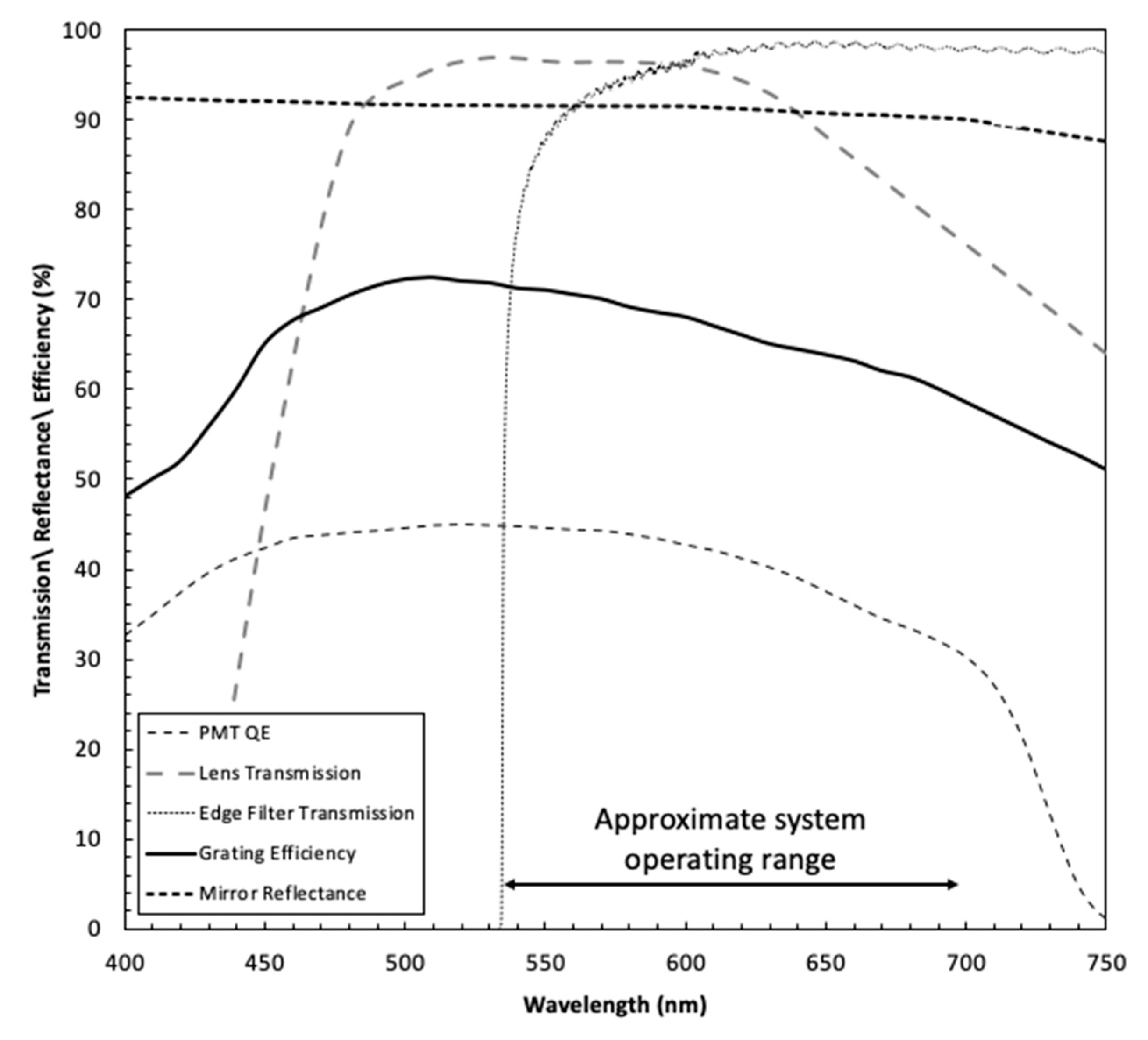
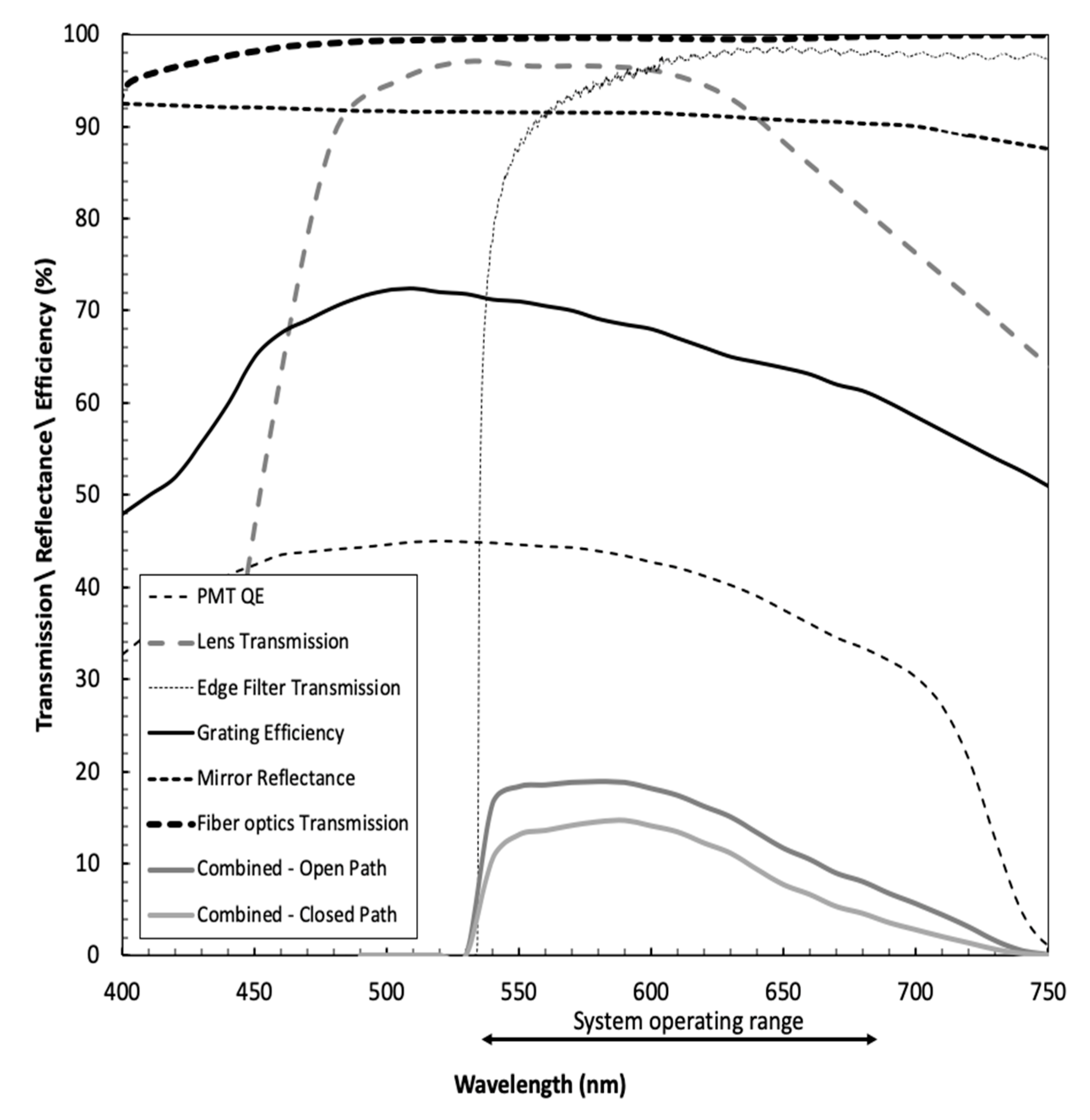
As noted above, multiple forms of dispersive devices can be employed in a Raman system. The two main categories of devices that garner the greatest attention are monochromators and spectrometers. As noted in Table 1, monochromators make use of moving (typically rotating) dispersive optics to scan a spectrum and to observe selected spectral bands at a narrow exit. In contrast, spectrometers, which often have fixed optics, simply disperse an optical spectrum across a broader exit opening, creating an image on the exit plane. Both categories of device, regardless of their specific design, make use of mirrors and gratings to guide and diffract light.

4.5.1. Mirrors

Once light enters a dispersive device, it will, as noted earlier, be directed across one or more mirrors. Like filters, mirrors also have a finite range over which they effectively reflect light. Here, the reflectance properties of the mirror (reflectance as a function of wavelength) will impact which wavelengths reach the exit of the dispersive device and thus the detector. Generally, mirrors are selected to effectively transmit the bulk of wavelengths in the desired Raman spectrum. However, Raman shifts that may occur near the boundaries of performance of the mirror may be lost in the observed spectrum, and mirror reflectance is often highly nonlinear at its limits. As a result, determination of reflectance is not simply about whether the mirror reflects a wavelength of interest but rather whether Raman scattering at a given wavelength is of an intensity great enough that it can still be observed after losses associated with diminished reflectance at the boundaries of the mirror reflectance range. The spectral region that can be observed after reflectance from a mirror is thus inherently related to the intensity of the observed light as a function of wavelength. Nonetheless, the mirror’s transmission curve is an important starting point for this evaluation.

4.5.2. Grating

The primary function of a dispersive device is enabled by one or more diffractive optics, termed gratings [37]. Multiple types of diffraction gratings may be encountered, for example, transmission, reflective, blazed ruled (several variants), echelle, and holographic. The wavelength transfer function is affected by the efficiency of the grating, which is a function of wavelength. Gratings are often optimized for a particular wavelength band, with peak efficiency for ruled gratings occurring at what is termed their blaze (typically reported in n m ). Transmission through the monochromator will thus be defined by the range of wavelengths over which the grating achieves a tolerable level of efficiency.

4.6. Detector

As noted above, three primary types of detectors are employed in Raman systems: PMTs, CCDs, and APDs. These devices are effective only over finite spectral ranges, as defined by their efficiency curves, which are a byproduct of the detector’s window composition, optical transducer element, and gain electronics. The device efficiency will thus influence the upper and lower boundaries (cutoff limits) of observable wavelengths for any system.

4.7. Effective Spectral Bandpass

Ultimately, while the wavelengths of Raman scattered energy depend upon the sample under investigation, the observable wavelength bandpass of a Raman system is a function of the combined efficiency of its optical train and is thus inherently linked to it intensity transfer function and the product of component efficiencies encountered along the light path through the system. It is therefore important to superimpose the transmission or reflection efficiency curves of the primary system components outlined above to see the composite effect of these components as a function of wavelength on the observable Raman spectrum. This process is illustrated in Figure 5. Definition of tolerable transmission levels as a function of wavelength is dependent upon the sensitivity desired from the apparatus and the needs of a particular experiment. Those transmission levels that are acceptable for the application being pursued define the system’s effective spectral bandpass. Obviously, it is most critical that the target Raman lines of the analytes of interest fall within the bandpass of the system, preferably in spectral regions of highest efficiency.

4.8. Wavelength Resolving Power

The ability of a Raman spectroscopic system to distinguish between two adjacent Raman shifts of the same intensity is termed the system’s limit of resolution. This limit is primarily driven by the characteristics of the dispersive device used in the system, particularly the minimum achievable slit width or, less commonly, the diffraction grating, with the poorer of the two driving practical applications. Employing the Rayleigh criterion for resolution, diffraction-limited resolution of a grating [37,38], which is wavelength dependent, is achieved when the first diffraction minimum of the image of one Raman return coincides with the maximum of another. The grating diffraction resolution limit Δ λ can thus be expressed as
Δ λ = λ m N = λ m G W  
where λ is the wavelength of interest (nm), m = 1 (the diffraction order, taken as 1 for the Rayleigh criterion), N   is the number of grooves illuminated, G is the groove density of the grating (lines/mm), and W is the illuminated width of the grating (mm). In Equation (44), m N is defined as the chromatic resolving power ( R ch ).
While the grating resolution limit is important to determine, its optimal performance can only be achieved if it is housed within a dispersive device of equivalent or better linear dispersion, D L [37,38]. This device-specific resolution limit is determined at the device plane of exit and is the product of instrument focal length, f i (mm), and angular dispersion, D A [37,38], where angular dispersion is the change in the diffraction angle d β corresponding to a change in wavelength d λ . Thus,
Angular   Dispersion   D A = d β d λ = G m cos β
Linear   Dispersion   D L = f i D A = f i ·   d β / d λ
Incorporating the properties of the dispersive device, this can be rewritten as
D L = f i · d β d λ = G m f i c o s β
where
G = groove density (number of grooves per mm)
m = order of diffraction ( m = 0, ±1, and ±2)
β = the diffraction angle, in degrees (the angle between the diffracted light and the normal to the grating)
To understand the instrument limit on wavelength resolution, one can invert Equation (47) to define the reciprocal linear dispersion, in nm / mm :
D R = c o s β G m f i
Multiplying D R by the width, W s (mm) of the exit slit provides an indication of the practical limit on wavelength resolution R s (nm).
R s = D R W s
From the above equations, a higher resolution can be achieved by either using smaller slits or by having a longer instrument focal length.

4.9. Summary of the Wavelength Transfer Function in a Raman System

The wavelength transfer function defines the wavelength bandpass and resolution of a Raman spectroscopic system. While the laser source characteristics and sample under investigation inherently shape the Raman spectrum to be observed, the elements of the optical train employed to collect, disperse, and detect the scattered radiation ultimately define what wavelength bands are observable. The transmission efficiency of filters (and fiber optics (if employed)), reflectance efficiency of mirrors and gratings in the dispersive device, and spectral sensitivity and gain of the detector, all as a function of wavelength, collectively define the bandpass of the instrument, with tolerable transmission levels at any given wavelength varying based on the goals of any given experimental activity. The resolving power of the system, in contrast, is typically driven by the characteristics of the dispersive device. The diffraction resolution limit of the dispersive instrument grating and reciprocal linear dispersion defined by the geometry of the dispersive instrument and choice of slit width compete to define the ultimate limit on wavelength bands that can be differentiated. In addition, this resolution limit establishes the uncertainty associated with any wavelength determination as R s .

5. Transfer Function: Time

The importance of the influence of Raman system components on the temporal characteristics of Raman observations varies based on Raman system design. There are generally two major categories of Raman instruments: (1) those that are integrative in nature and thus accumulate observations at any given wavelength over a desired period of time and (2) those that are time-resolved and thus employ gating technologies to carefully select time intervals of observation. Continuous wave (CW) lasers are typically employed for the former, while pulsed lasers are usually employed for the latter. As the integration times for CW systems are typically straightforward to define and the time required for light to traverse the optical path of an open-path Raman system is generally negligible, this discussion will focus on time-resolved pulsed laser systems as well as the effects of fiber optic elements that may be utilized in a closed path system.

5.1. Optical Fibers

In a closed-path Raman system, optical fibers are used to guide light. As noted earlier, single-mode fiber is typically used to guide the narrow-band source energy to the sample; however, given the varying spectral characteristics of Raman returns and desire to collect as much Raman scattering as possible, multi-mode optical fiber is usually used for collection.
There are three primary ways in which fiber optics influence the time characteristics of a Raman system: modal dispersion (distortion), material chromatic dispersion, and waveguide dispersion [38]. Modal dispersion stems from electromagnetic wave mode-dependent differences in propagation path length through a fiber as the light enters the fiber at different incidence angles, which results in different transit times for different modes. Similarly, material chromatic dispersion results from variations in the refractive index of the fiber core as a function of wavelength, which again lead to differences in path lengths and thus transit times. Finally, waveguide dispersion, which is another form of chromatic dispersion, stems from the wavelength-dependent distribution of mode power between the core and cladding of the fiber, which have different refractive indices and thus transit speeds. Note that polarization mode dispersion will be ignored here as its effects are typically about two orders of magnitude less significant than the other influences described. With the exception of ultra-short pulse systems, it will be negligible over the typical fiber lengths employed in a closed-path Raman system. Phase delay is also not discussed here as it is primarily relevant in advanced nonlinear Raman imaging applications, which are beyond the scope of this analyses.

5.1.1. From Excitation Source to the Sample

When a laser is incident upon a sample in a closed path fiber optic system, depending upon the transit distance in the fiber from the laser source to the sample, some pulse broadening [39] due to material chromatic dispersion of the source linewidth may occur. This is because even a laser’s output has a finite spectral linewidth, σ λ 0 , and there are likely to be propagation delays associated with the varying components of the source energy, as the different spectral components will have different group velocities [40].
Group velocity, V g (m/s) can be defined as
V g = ω f k f = c n f λ center ( d n f d λ center )
where ω f   is the light wave’s angular frequency (radians/s), k f is the (angular) wavenumber (radians/m), c is the speed of light in a vacuum (m/s), n f is the bulk fiber refractive index at the pulse center wavelength λ center (nm), and d n f d λ center is the change in refractive index of the fiber with respect to a change in wavelength (e.g., corresponding to the spectral range represented by the source linewidth).
Thus, the group delay, t g (i.e., the time in seconds for the group to traverse fiber of length, l fiber , in meters), is given by
t g = l fiber V g
Then, for a pulse of spectral width σ λ 0 , the pulse broadening due to material chromatic dispersion, Δ t material , in seconds, can be estimated by
Δ t material = d   t g d   λ o σ λ 0 = D mat · l f i b e r · σ λ 0
where D mat is the material dispersion coefficient, typically reported in units of time/spectral width per kilometer of fiber. In addition, waveguide dispersion is also likely. Waveguide dispersion is often represented by a similar coefficient, D wgd , which is calculated by considering an effective refractive index ( n eff ) to account for variations in the propagation constant across the fiber core and cladding for different wavelength components of the propagated mode.
For a pulsed source of wavelength λ center , with a linewidth of λ center ± Δ λ 2 , pulse broadening in a single mode fiber will be affected primarily by the above-outlined dispersion effects and will be the sum of the material chromatic dispersion broadening, Δ t material , and the waveguide dispersion broadening, Δ t waveguide   [41]:
Δ τ SMF = Δ t material + Δ t waveguide

5.1.2. From the Sample to the Dispersive Device

Because Raman photons stem from effectively immediate scattering of the excitation source, Raman scattered light collected in a closed path multi-mode fiber system can only exist when the laser pulse is on and will thus also be recorded as a pulse that is subject to broadening over the return path to the system optical dispersive device. On the collection path, however, the spectral width of the collected light for which these effects must be accounted is far broader than on the excitation path, and thus time delays that are wavelength and mode dependent have the potential to be more significant.
Material chromatic dispersion and waveguide dispersion (to a much lesser extent) will again be present in a closed path collection fiber. Rather than bounding the effect based on the spectral linewidth, in the case of Raman returns, it is important to understand the minimum and maximum wavelengths that bound the sought-after Raman spectrum. Once defined, Equations (52) and (53) described above can again be used to determine the temporal spread in photon arrivals that can be expected across the Raman spectrum.
In addition to chromatic dispersion factors, variations in the temporal characteristics of the optical returns will also stem from modal dispersion [42]. The different modes of the collected light, even if of the same wavelength, will travel at different velocities within the fiber, leading to distortion of the output relative to the input over distance. The pulse broadening resulting from modal dispersion can be determined by considering the difference in the transit times of the zero-order mode (light effectively traveling down the central axis of the fiber) and the highest-order mode (light undergoing total internal reflection at/near the critical angle of acceptance of the fiber, θ c ).
The transit time for each mode will simply be a function of path length of the mode in the fiber divided by the velocity of the mode. The former is a function of fiber’s physical length, l fiber , and the angle, θ a , relative to the fiber axis. The latter is a function of the refractive index of the material through which the mode propagates. With these inputs, the transit time for a given mode is
t mode = d i s t a n c e v e l o c i t y = l fiber / cos θ a c / n = l fiber · n c cos θ a
Thus, the transit time for the lowest order mode ( θ a = 0 ) is given by
t min = l fiber · n core c
Then, building on Snell’s law of refraction, for the critical angle, θ c , at the fiber core-cladding interface is
cos θ c = sin ϕ c = n cladding n core
where ϕ c is the angle of critical ray incidence relative to the core-cladding normal.
Thus,
t max = l fiber · n core 2 c · n cladding
and the total delay difference, i.e., pulse broadening, is given by
Δ t modal = t max t min
As chromatic dispersion and modal dispersion are independent of each other, they are combined as a sum of squares [42], so that the total delay difference for the two effects is
Δ τ MMF = ( Δ t material + Δ t waveguide ) 2 + Δ t modal 2
Of course, before presuming any of the above outlined potential effects on the time characteristics of the delivered and observed optical energy in a Raman system, it is important to determine if any dispersion-compensating fibers are being employed, which can help mitigate the effects described above.

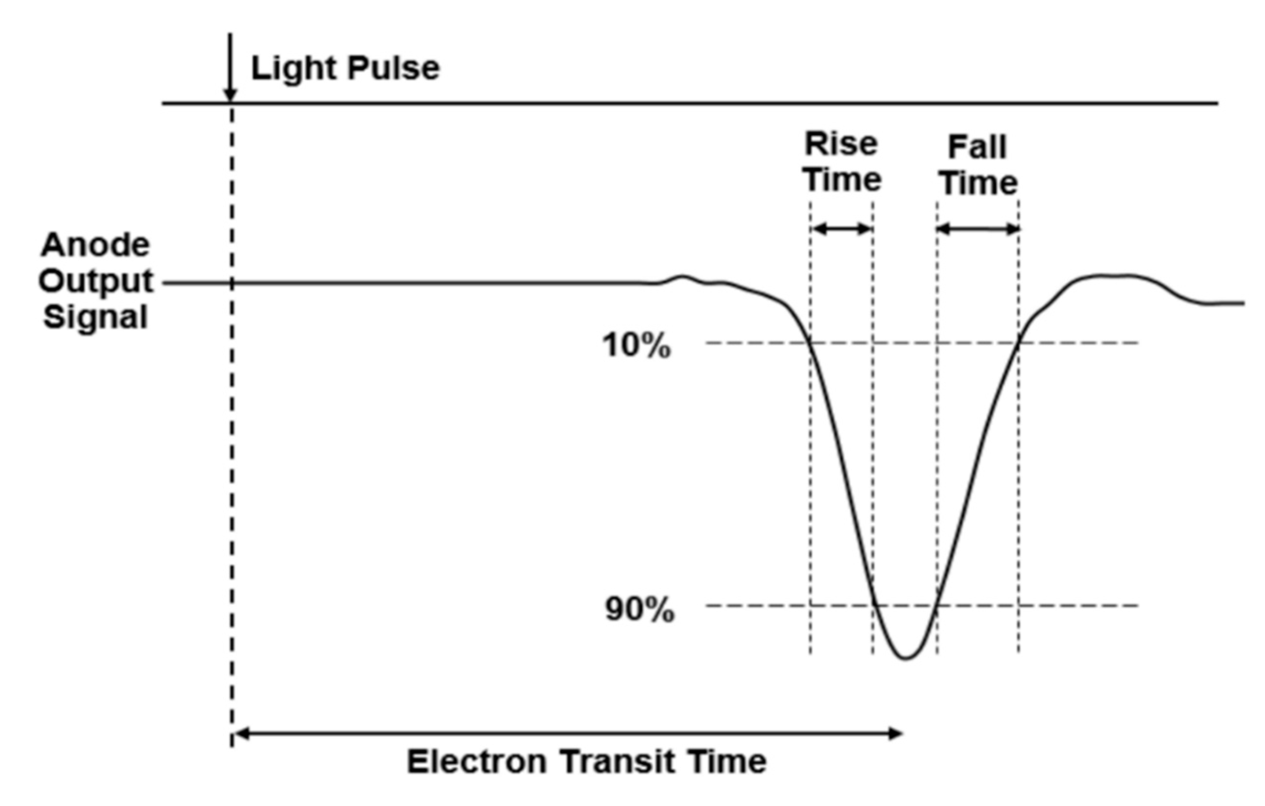
5.2. Detector Response Time

While different wavelengths may indeed travel over different path lengths in some dispersive devices, the variations in path length are likely far too small to be of significance in most Raman systems. Thus, the examination of influences on the temporal characteristics of the Raman system’s collection side will now turn to the detector and, in particular, examine the optical to electrical conversion that must take place to record Raman observations electronically. Each of the detector alternatives described in the intensity discussion can again influence the temporal characteristics of what will now become an electronic signal.

5.2.1. PMT

As the photons enter a PMT, it takes time for the electrons (or photoelectrons generated when the photons hit the cathode) to reach the anode. This time response is a primary function of the PMT dynode geometry and supply voltage. Figure 6 [25] helps define the important time characteristic of a PMT anode response. The electron transit time is the time interval between excitation at the PMT photocathode and the peak of the anode response. The rise time refers to the time for the anode signal output to increase from 10% to 90% of the maximum. Conversely, the fall time is the time it takes for the anode output to decrease from 90% to 10% of the peak. The fall time is often 2 to 3 times that of the rise time. Thus, the PMT transit time amounts to a time delay in the transfer function of the system. In time sensitive analyses, such as time resolved photon counting, it is preferable that the fall time be sufficiently short to prevent overlap with the next photon arrival.
In addition to transit time delay, transit time spreading can also be an important parameter in time-based measurements. Transit time spread refers to the inherent variability in the transit time of the PMT over multiple non-coincident photon arrivals and is typically recorded as the FWHM (Full Width at Half Maximum) of a histogram of these observations. The transit time spread provides insight into the uncertainty in the time resolution of the PMT measurement system.

5.2.2. APD

The mechanism to generate photocurrent in an APD is similar to other regular photodiodes. The time delay of an APD can be characterized by its response time and rise time. The response time, which amounts to a delay in the measurement system, is defined as the time required for the detector to respond to an optical input, as it takes time for the semiconductors in the photodiode to generate electron-hole pairs and resulting current. This parameter is the root mean square sum of three components [26,29]: the resistance-capacitance ( R APD C APD ) time constant, diffusion time for filling the depletion layer in the photosensitive area, and the carrier transit time in the depletion layer. The RC time constant ( τ RC = R APD C APD ) , which stems from the resistance ( R A P D ) and capacitance ( C APD ) of the photodiode circuit, often lengthens the photodiode impulse response. It is the time for the detection circuit to charge the capacitor through the resistor, from a voltage of zero to 63.2% ( 1 e 1 ) of the final steady state reading voltage. The rise time of the APD has an identical definition as is in the previous discussion of the PMT.

5.2.3. CCD

The time delay in a CCD is influenced by two factors: the integration time and read out time [26,27]. Image generation in a CCD typically occurs in four stages, including: (1.) photon–photosensitive region interactions that generate charges, (2.) charge collection and storage, (3.) charge transfer, and finally, (4.) the charge measurement. The stored charge on a device pixel is usually linearly proportional to the number of incoming photons (light flux) until the well capacity is achieved. Depending on the light flux arriving at the CCD, different integration times (exposure time) can be employed to accumulate charge. The charge-transfer process and the charge-measurement algorithm collectively influence the readout time and are crucial to the time efficiency of a CCD. CCDs are generally several orders of magnitude slower in response time than PMTs or CCDs and thus are typically used in an integrating mode.
Note that time and fall time characteristics of the detector transit time will also inevitably result in distortion of the intensity-time profile of the observed response relative to the actual phenomenon under investigation.

5.3. Coaxial Cable Delay

Signals obtained through the optical-to-electrical conversion offered by optical detectors are typically conveyed to a data acquisition system via some form of cabling, the most common of which is coaxial cable [43,44]. When an electrical signal travels through a 50 Ω impedance coaxial cable, its speed V cable [45] can be expressed as
V cable = 1 L C cable
where L and C cable are the inductance and capacitance per meter length of the coaxial cable. An RG-58 cable has roughly 0.2–0.3 μH/m inductance and 90–100 pF/m capacitance and thus has a signal travel speed of 1.98 × 10 8   m/s. In a Raman system, there are usually two sets of cables: one connects the PMT to an amplifier, and the other connects the output of the amplifier to the data acquisition card in the computer. For the total cable length l cable (m), there will be a delay t cable (s) due to signal transmission:
t cable = l cable / V cable
In addition, the amplifier itself is likely to impart at least some transit time delay on the system output. These delays are especially important in a pulsed laser time-resolved detection setup, as it is often desirable that the data acquisition unit (DAQ) be configured to acquire data only when the laser pulse is on, requiring synchronization of a trigger and observation times to minimize acquisition of unwanted noise. Generally, when a cable is used for signal transmission in a Raman spectroscopic system, it should be as short as possible.

5.4. Summary of the Time Transfer Function in a Raman System

Time effects in Raman spectroscopic systems are most pronounced in time-resolved experiments. Primary sources of delay and potentially of pulse shape distortion stem from propagation delays in the fiber optics of closed path systems, transit times of detectors, and inevitable transmission delays in electrical conduits. In addition, devices impart statistical variation in transit times that can limit time resolution in experiments.

6. Purdue CE Spectroscopy Lab 532 nm TRRS

Building on the in-depth discussion of the factors that contribute to Raman system transfer functions in intensity, wavelength, and time, this section details an example transfer function analyses, contrasting open-path and closed-path versions of a 532 nm excitation wavelength Time-Resolved Raman Spectroscopy system (TRRS) in the Purdue University Civil Engineering Spectroscopy Lab. An overview of each system configuration is provided in Section 6.1 and is illustrated in Figure 7. This is followed by in-depth analysis of the open-path system in Section 6.2, the closed-path system in Section 6.3, and a brief discussion of the analyses in Section 6.3.

6.1. System Description

6.1.1. Open-Path System

Details of the open-path Purdue TRRS system have been reported previously [46,47,48]. In this setup, a time-resolved Raman spectroscopic system (TRRS) was designed to facilitate analyses of chemicals in aqueous solutions. The optical path aims to allow 180° collection of the Raman scattered returns. In this experiment setup (Figure 7), a {1} 3 μJ/pulse laser is used for excitation and the Raman photons are collected through a series of lens, mirrors, filters, and a monochromator, before finally reaching a PMT. The laser has a 5.6 kHz repetition rate and <900 ps pulse duration and a beam waist radius of 649 μm. The excitation beam is incident onto a dichroic mirror {2} at 45° to split the beam in two directions. Part of the beam (10%) goes to a plano-convex lens {6} to establish a photodiode trigger {11} that primes the data acquisition system, and the other part passes through an aspheric lens {3} to focus the beam on the sample which is housed in a cuvette {4}. The Raman photons from the sample pass through the aspheric lens {3}, which collimates the collected scattered light and directs it toward an achromat {5} that focuses the beam at the entrance slit of the monochromator (1/8 m monochromator with 1200 lines/mm, 30 mm wide grating) {8}. A 532 nm long-pass filter {7} is installed in front of the monochromator slit to remove the unwanted 532 nm radiation. After traversing the monochromator, light is incident upon a PMT {9}. The PMT output first goes through an amplifier {10} with a gain factor of 20× before transmitting to a data acquisition unit {12}. Overall, the specific optical path is {1} → {2} → {3} → {4} → {3} → {2} → {5} → {7} → {8} → {9}. Part of the excitation beam goes through {2} → {6} → {11} to the photodiode to trigger the data acquisition unit.

6.1.2. Closed-Path System

Details of the closed-path variant of the system have been reported previously [13,48]. This setup (Figure 7b), like the open-path configuration, was designed to facilitate analyses of chemicals in aqueous solutions. The optical path allows 180° collinear backscatter collection using a fiber-optic Raman probe {16} that contains a series of built-in optics. On the in-bound path, the Raman probe guides light through a 105-μm core single-mode fiber to a collimating optic, bandpass filter (for the laser line), dichroic mirror, and an exit optic with a 7.5 mm focal length which focuses excitation energy on the sample. Raman scattered returns are then collected back through the probe focusing optic, directed off the internal dichroic mirror and a standard mirror to change their path to that of the collection fiber, and then traverse a long-pass filter (to remove Rayleigh and anti-Stoke scattering) and optic which couples the return into a 200-μm core multi-mode fiber. As shown in Figure 7, this setup shares many components with the open-path design but makes use of the fiber-optic Raman probe in place of the optics on both the inbound and outbound optical trains of the open-path system and utilizes a different monochromator. In-bound laser light is coupled into the fiber optic probe using an objective lens {13}. An f-matched coupler {14} directs light from the outbound fiber into a 1/8 m monochromator {15}. Overall, the specific optical path is {1} → {2} → {13} → {16} → {4} → {16} → {14} → {15} → {9}. Similar to the open-path system, part of the excitation beam goes through {2} → {6} → {11} to a photodiode to trigger the data acquisition unit.

6.2. Open-Path Sample Calculation

Herein, the equations developed in the previous sections of this paper are applied, as relevant, to the open-path Purdue TRRS system. For the purposes of this analysis, water is assumed as an analyte with a particular emphasis on the Raman return of representative of the O–H stretching band, which manifests at 649.98 nm. The following considerations have been incorporated in this analysis, which are organized here by the optical path through the system:
Excitation:
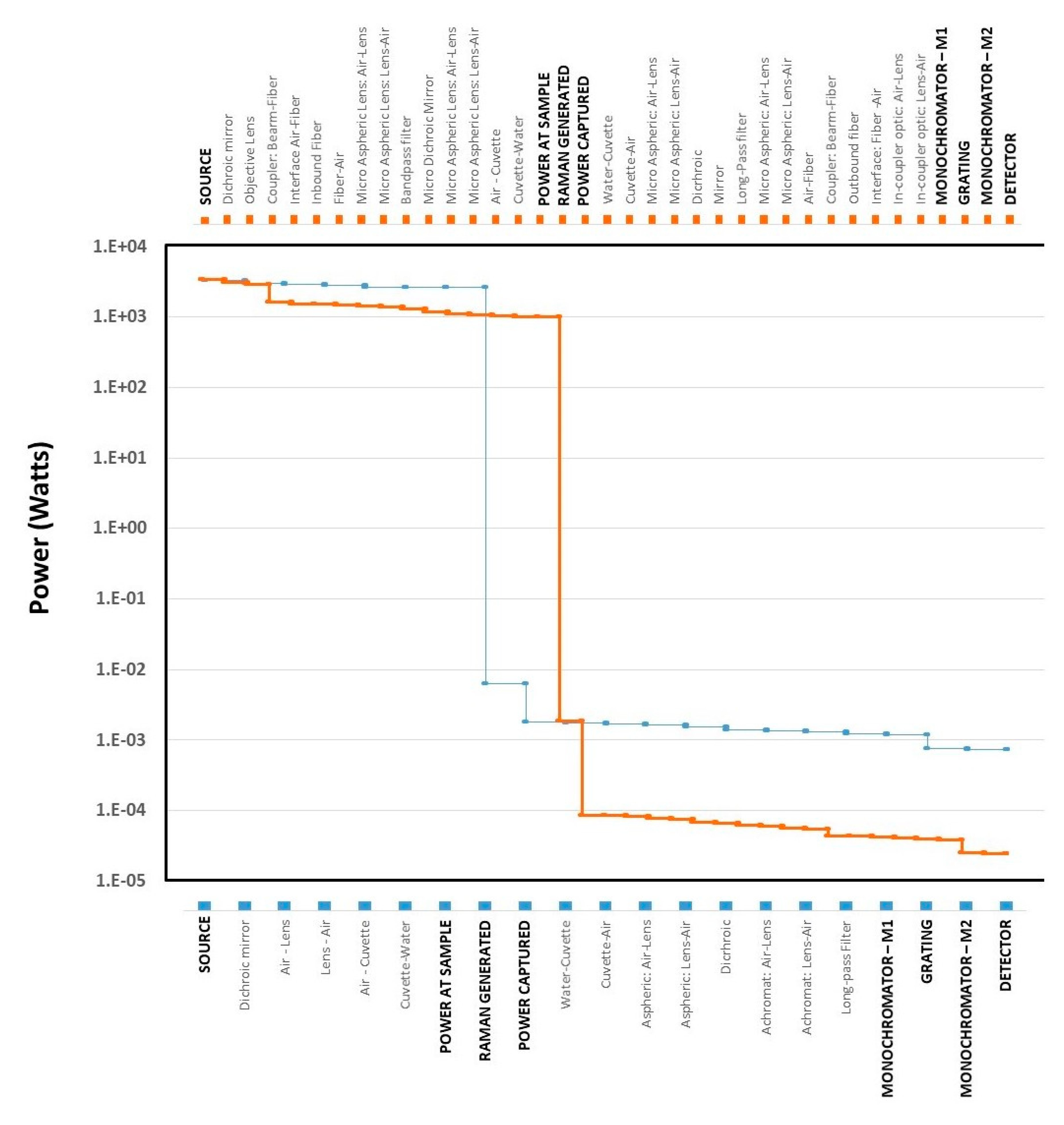
  • Equations in Table 2 have been employed to characterize the intensity of the laser source (Component {1} of the TRRS system) on a per pulse basis.
Inbound Path:
  • Equations from Table 3 have been employed to define the intensity characteristics of the system on the inbound optical path to the sample, which contains one dichroic mirror {2} and one aspheric lens {3}.
  • Due to the simplicity and open-path nature and careful optic selection of the Purdue TRRS system, no effects on time or wavelength are identified on the inbound path to the sample.
  • The time characteristics of the system are defined by the inbound path length of 20 cm.
Sample:
  • Equations from Table 4 have been employed to characterize Raman scattering achieved in the sample cuvette {4}. As noted above, for the purpose of this example, the sample is defined as water and observations are focused on 649.98 nm with a Raman cross section equal to 7.29 × 10⁻²⁹ cm2molecule−1 49].
Outbound Path:
  • Equations from Table 5 have been employed to assess intensity effects on the outbound path which includes one aspheric lens {3}, the dichroic filter {2}, one achromat {5}, and one long-pass filter {7}.
  • The wavelength transfer function is affected by the long-pass filter {7} in this stage of the system.
  • The time characteristics of the system is defined by the outbound path length of 25 cm.
Dispersive Device:
  • Analysis of the intensity through the monochromator {8} in the system employs the equations in Section 3.4, which account for the mirrors and grating in the device.
  • The wavelength transmission effects are directly linked to the mirror and grating characteristics of the system using equations articulated in Section 4.5.
  • Transit time is estimated by the configuration of the monochromator.
Detection and Acquisition Electronics:
  • The output measures conveyed in the intensity analysis detailed in Table 7 are presented as a function of the total power at a given wavelength, λ, and then as a function of the number of photons at the wavelength λ. Power distribution cross the Raman spectrum is not specified.
  • Equations detailed in Table 6 are employed to define the output intensity of the PMT {9}, and equations from Section 3.6, Section 3.7, and Section 3.8 are employed to define the intensity-related effects of the coaxial transmission cables, the amplifier {10}, and the data acquisition system {12}.
  • The wavelength transfer function is most notably affected by the PMT {9} quantum efficiency curve in this stage of the system, as described in Section 4.6.
  • Temporal effects in this stage of the system stem from transit delays in the PMT {9}, Amplifier {10}, and interconnecting cables as discussed in Section 5.3, as well as transit time spread in the PMT {9}.
Table 7, Table 8 and Table 9 detail the application of the above considerations to the Purdue TRRS system for intensity, wavelength, and time, respectively.

6.3. Closed-Path System Sample Calculation

Excitation:
  • As for the open-path system, the equations in Table 2 have been employed to characterize the intensity of the laser source (component {1} of the closed-path TRRS system) on a per pulse basis.
Inbound Path:
  • The equations from Table 3 have been employed to define the intensity characteristics of the system on the inbound optical path to the sample, which contains one dichroic mirror {2}, one objective lens {13}, the in-bound fiber leg of the Raman probe, and the optical components built into the Raman probe {16}, which include an aspheric lens, bandpass filter, dichroic mirror, and focusing lens.
  • Again, due to careful optic selection and use of low-OH fiber in the Raman probe {16}, no effects on wavelength are identified on the inbound path to the sample.
  • The time characteristics of the system are defined by the inbound path length, including the in-bound fiber leg of the Raman probe.
Sample:
  • The calculation is similar to the open-path system discussion but with a different path length of the laser in the sample (dz) and notably different scattering collection (λ). Equations from Table 4 have been employed to characterize Raman scattering achieved in the sample cuvette {4}. As noted above, for the purpose of this example, the sample is again defined as water and observations are focused on 649.98 nm with a Raman cross section equal to 7.29 × 10⁻²⁹ cm2molecule−1 [49].
Outbound Path:
  • The equations from Table 5 have been employed to assess intensity effects on the outbound path which includes the outbound fiber leg of the Raman probe as well as its internal optics on the return path one micro aspheric lens, one dichroic mirror, one standard mirror, one long-pass filter, and a coupling optic {16}.
  • The wavelength transfer function is affected by the long-pass filter in the probe in this stage in a manner identical to that in the open-path system.
  • The time characteristics of the outbound path are defined by the outbound path length and fiber optic leg of the Raman probe {16}.
Dispersive Device:
  • Analysis of the intensity through the monochromator {15} in the system employs equations in Section 3.4, which account for the mirrors and grating in the device.
  • The wavelength transmission effects are directly linked to the mirror and grating characteristics of the system using equations articulated in Section 4.5.
  • Transit time is estimated by the configuration of the monochromator.
Detection and Acquisition Electronics:
  • As the components in this part of the system are identical to those in the open-path system, they will not be reanalyzed here and reference can be made to the previous discussion in Section 6.2.
Table 10 and Table 11 detail the application of the above considerations to the closed-path Purdue TRRS system for intensity and time, respectively. Note that wavelength effects are examined in the discussion below but do not differ from the open-path system enough to justify presentation in tabular form.
In addition, Figure 8 depicts the effects of the inbound- and outbound-path optics, the monochromator’s grating and mirrors, and the PMT’s quantum efficiency on the overall effective wavelength bandpass of the system and relative intensity effects as a function of wavelength. For contrast, the composite curve for the closed-path system is also shown. Note that careful choice of optics and use of low-OH fiber in the fiber optic probe of the closed path system as well as use of efficient mirrors and gratings in the monochromator of the closed-path system yield a similar operating range to the open-path system.

6.4. Discussion of Transfer Function Analyses

Assessment of the intensity, wavelength, and time transfer functions of the TRRS systems described above provide several important insights. When considering intensity in the open-path system, it is apparent that a very small fraction of incident energy has the potential to be detected as Raman scattering, underscoring the fundamental challenge of Raman analysis. In addition, the intensity analysis highlights that even small losses from transmission through optics can add up and thus system designs that err toward simplicity have inherent advantages. This said, the greatest contributions to intensity loss in the open-path example system relate to the collection efficiency of the optics employed to capture Raman scattering and the efficiency of the monochromator grating and to the overall quantum efficiency of the detector, which in this case is a PMT. In contrast, in the closed-path system, use of the fiber probe significantly reduces attainable intensity for any given input, as losses incurred upon coupling the laser into the fiber as well as those resulting from traversing the fiber and numerous built-in optics are significant. In addition, the limited numerical aperture of the probe focusing/ collection optics hinder scattering collection. As illustrated in Figure 9 and by comparing I Dispersed Out or the power incident upon the detector detailed in Table 7 and Table 10 for the two systems, the open-path setup is approximately 30× more effective in terms of observable scattering than the closed path system.
In terms of the wavelength transmission characteristics of the open-path system, combination of the long-pass Rayleigh filter (to remove the laser line), monochromator bandpass, and PMT efficiency yield a narrow envelope of wavelengths for which signals of an acceptable intensity can be observed and wavelength resolution is fundamentally limited by the monochromator—a choice that must be defined at the outset of experimental design. This is also the case for the closed-path system, which displays very similar bandpass characteristics to the closed-path system Temporally, while there is substantial delay in the open-path system as electrical signals traverse the PMT, amplifier, and cable interconnections, it is the transit time spread of the PMT that is likely to have the most adverse effects on photon detection for the system as this spread sets the limit on the pulse-to-pulse differentiation required to enable effective photon counting. Although not influential on performance limits of the system, the time delay in the design is critical to define to effectively gate and mode lock data acquisition with the laser pulse rate and thus to effectively reduce capture of stray light. In contrast, in the closed-path system, transit time effects are significantly influenced by the fiber components of the system, driving increased overall system transit time, pulse broadening, and slight temporal dispersion of wavelengths. While overall time delay is again inconsequential, pulse broadening and temporal dispersion of wavelengths could become significant when a fiber coupled system is employed to interrogate samples at significant distances from the excitation source and/or detector (e.g., in some industrial process applications) and must be accommodated by recognizing the variation in scattered return wavelengths as a function of arrival time and by limiting pulse-to-pulse detection timing.

7. Conclusions

Over the past several decades, Raman spectroscopy has proven to be an efficient way to obtain insight into the chemical composition of different forms of matter, serving an array of applications in chemistry, environmental science, biological science, food science, medicine, security, forensic science, agriculture, industrial process monitoring, and many other fields. While instruments have historically been large and complex, advances in technology have yielded Raman systems that are now small, affordable, and often user friendly, further expanding the population employing Raman methods.
Although each experiment setup is different and some of the parameters in a system may be challenging to determine, the discussion and example development of system transfer functions outlined herein are intended to aid those who want to gain sufficient knowledge and understanding to assess their own system’s capabilities, to tailor application of the Raman technique for specific uses, to identify areas for optimization or modification of otherwise off-the-shelf equipment, or even to interpret the results put forward by other researchers with different instruments. This article systematically explores the ways in which the specific components and configurations of a Raman system affect its performance along three principal dimensions: intensity, wavelength, and time.
On the dimension of intensity, optics, filters, dispersive device characteristics, and detector performance have the greatest influence on open path systems. When operated in a closed path configuration, fiber optic losses can also be substantial. Careful forethought about the spectral range that is to be examined in any given application is critical to ensure optic transmission, mirror reflectance, grating blaze, and detector efficiency are optimized for best results. Of course, the fewer variations in refractive index across a system optical train, the stronger the likely output. Resolution of the signal generated by Raman scattered returns is ultimately a byproduct of the detector sensitivity and data acquisition unit bit count.
For the wavelength, variations in throughput in an open path system stem primarily from filter choices, dispersive device characteristics, and detector efficiency. These variables must be considered cumulatively and yield an envelope (band) of performance for which light can be detected at acceptable levels for any given experiment. Closed path systems encounter additional complications as a result of the transmission characteristics of fiber conduits, and thus, fiber must be selected carefully. Regardless of the system design, wavelength resolution is inevitably limited by the poorer of the dispersive device’s grating diffraction limit or reciprocal linear dispersion.
In terms of time, the length of the electrical transmission cables and detector transit time have the greatest effects in an open-path system. In contrast, the length of optical fibers in a closed-path system plays an important role, particularly in time-resolved experiments that could suffer from chromatic and/or modal dispersion. While time delays are critical to understand, they can typically be accommodated. However, temporal spreading can be of concern and can irreparably distort output observations. As in any time-based experiment, the detector, amplifier, transmission electronics, and the data acquisition unit should be appropriately selected to accommodate anticipated signal frequencies (electrical bandwidth).
As Raman spectroscopy and especially the use of compact Raman spectrometers becomes more and more popular, understanding the performance benefits and limitations of different components and system designs is critical to facilitate experiment design and interpretation of results. The types of analyses discussed herein stem from perspectives put forward in a wide array of fundamental literature and span concepts from physics, analytical chemistry, electronics, and photonics, among others. For an individual researcher, gathering these perspectives can be challenging as even in most texts focused on Raman spectroscopy nearly the entire scope of this paper falls into one parameter that is often referred to as the instrumentation constant, a parameter that is often given little attention because it relates to systematic variation in outputs rather than test-to-test variation. However, as evidenced in the above analysis, numerous aspects of this instrumentation constant have significant implications on the quality and nature of results that can be obtained with any given instrument, the potential to customize or tailor a system, the ability of the instrument to be employed for different applications, and the potential to effectively compare results between instruments. Thus, understanding the system transfer function—particularly along the dimensions of intensity, wavelength, and time—is critical. It is hoped that the exposition of the variables influencing a typical Raman system transfer function put forward herein provide a guide to this very important analysis.

Author Contributions

Conceptualization, Y.-C.L. and J.V.S.; methodology, Y.-C.L. and J.V.S.; validation, Y.-C.L. and J.V.S.; formal analysis, Y.-C.L. and J.V.S.; writing—original draft preparation, Y.-C.L. and J.V.S.; writing—review and editing, Y.-C.L. and J.V.S.; visualization, Y.-C.L. and J.V.S.; supervision, J.V.S.; project administration, J.V.S.; funding acquisition, J.V.S. All authors have read and agreed to the published version of the manuscript.

Funding

This work was sponsored by the Purdue Civil Engineering Spectroscopy Laboratory.

Conflicts of Interest

The authors declare no conflict of interest.

Abbreviations and Symbols

A R a d i a t e d Radiated detector area cm 2
A in Area of the beam entering the optical train cm 2
A in Area of the beam entering the outbound optical train cm 2
A in Area of the beam on the coupling optic cm 2
A out Area of the beam exiting the optical train cm 2
A out Area of the beam on dispersive device coupling optic cm 2
A out Area of component immediately following dispersive device cm 2
APDAvalanche photodiodes
C A PD Capacitance in APD F   ( A 2 · s 4 kg · m 2 )
C cable Capacitance per meter length of the coaxial cable F   ( A 2 · s 4 kg · m 2 )
C CCD CCD output in counts for a given pixel
CCDCharge-coupled devices
C E PMT PMT collection efficiency
  C F ADU C CCD device specific analog-to-digital conversion factor linking generated photoelectrons to reported counts
C F ADU I CCD device specific analog-to-digital conversion factor linking generated photoelectrons to a pixel intensity
CWContinuous wave laser
c Speed of light m / s
D Density of scatters molecules / cm 3
D A Angular dispersion
DAQData acquisition unit
D E PMT PMT detection efficiency
D L Linear dispersion
D mat Material dispersion coefficientps/nm/km
D o Diameter of the inbound beam at the pre-sample focusing optic cm
D P APD APD photon detection probability
D R Reciprocal linear dispersion nm / mm
D wgd Waveguide dispersion coefficientps/nm/km
d a Illuminated spot size in the sample cm 2
d FP Diameter of the laser at the focal point cm
d z Path length of the laser in the sample cm
d β Change in the diffraction angle degrees
d λ Change in wavelength mm
E CW Energy emitted by a CW laser J
E electron Charge of an electron C
E P Energy emitted by a pulsed laser J
E pulse Average pulse energy of a pulsed laser J
E photon Energy of a photon J
  E Photon Energy (in Joules) of photons of the dispersed band at wavelength λ J
E Source Energy of the laser excitation J
e Euler’s number
F S DAQ full scale range V
f / # The ratio of the lens’ focal length to the diameter of the aperture
f F Focal length of the focusing lens cm
f i Dispersive instrument focal length mm
G Groove density of the grating lines / mm
G Amp Amplifier gain
G APD APD gain factor
G CCD CCD gain
G PMT PMT gain
h Planck’s constant Js
I 0 Incident laser intensity on the sample W / cm 2
I CW Intensity of a CW laser beam W / cm 2
I Dispersed In Intensity of light ultimately reaching the dispersive device W / cm 2
I Dispersed Out The radiation coupled into the dispersive device that ultimately transits to the detector (at the exit of the dispersive device), at a given wavelength, λ W / cm 2
I Inbound The intensity of light ultimately transmitted after traversing an optical train of components
I N T Rounding down the number to the nearest integer
I Outbound   Intensity of collected Raman scattering immediately outside the sample container W / cm 2
I P Intensity of a pulsed laser beam W / cm 2
I R Raman intensity Watts
I Source   Intensity of the laser beam W / cm 2
k f Angular wavenumber radians / m
L Inductance per meter length of the coaxial cable H   ( kg · m 2 s 2 · A 2 )
L C con Coaxial cable loss per cable connector dB
L cable Coaxial cable attenuation per unit length dB / m
L con Fiber optics connector loss dB
L f Fiber optics total loss dB
L fiber Fiber optics intrinsic loss/Fiber loss dB / m
l cable Fiber optics splice loss dB
l fiber Length of the coaxial cable m
L cable Length of the fiber m
MMFMulti-mode fiber
m Diffraction order
N DAQ DAQ bits
N Number of grooves illuminated
N con Number of linked connector pairs
N fiber Number of fiber segments
N g D Number of times the light interacts with gratings
N m D Number of times the light interacts with mirrors
N spl Number of splices
n e ff Effective refractive index
n f bulk fiber refractive index at the pulse center wavelength
n i . Material refractive index
PPulsed laser
PMTPhotomultiplier tubes
P CW Average power of a CW laser W
P Detector In ,Light power incident on the detector for a given wavelength (band) λ W
P P Average power of a pulsed laser W
p Detector In Number of photon arrivals per unit time at the detector
p source Number of photons emitted from the laser over time
p Threshold signal magnitude associated with a single photon
Q g D The efficiency (%) of the grating encountered at interaction
Q E APD APD quantum efficiency
Q E CCD CCD quantum efficiency
Q E PMT PMT quantum efficiency
R Reflectance
R DAQ Number of quantization levels
R APD Resistance in APD Ω
R a c Reflectance—air—container wall interface
R c a Reflectance—container wall—air interface
R c s Reflectance—container wall—sample interface
R ch Grating chromatic resolving power
R fib Reflectance of the fiber tip at the air-fiber interface
R Load PMT circuit resistance load Ω
R m Mirror reflectance%
R m D Reflectance of the dispersive device mirrors
R opt Reflectance of the lens
R s c Reflectance—sample—container wall interface
R s Practical limit on wavelength resolution nm
S APD APD photosensitivity A / W
S PMT PMT photocathode radiant sensitivity mA / W
SAPDSingle-photon avalanche diodes
SMFSingle-mode fiber
T Transmittance
T bs Beam splitter transmittance
T cable   Percentage transmitted in a coaxial cable
T Con in The percentage of the excitation energy from the exterior of the sample interface that reaches the sample on the other side
T fiber   Percentage transmitted of fiber optics
T fil Transmittance of the filter
T opt Transmittance of the lens
t cable Signal transmission delay in a coaxial cable s
t g Group delay s
t max Transit time in fiber optics, highest order s
t min Transit time in fiber optics, lowest order s
t mode Transit time in fiber optics s
tonLaser on times
t pulse Pulse width of a pulsed lasers
V Acquired   DAQ output voltage V
V APD I APD output voltage V
V cable Electrical signal speed m / s
V CCD CCD output voltage V
V Detected   Detector output voltage V
V g Group velocity m / s
V Max   Maximum values of the full-scale output V
V Min   Minimum values of the full-scale output V
V Out   Signal that ultimately reaches the data acquisition unit V
V photon Voltage threshold representative of a photon arrival V
V PMT PMT voltage output
W Illuminated width of the grating mm
W s Exit slit width mm
β Diffraction angle degrees
γ laser Repetition rate of a pulsed laser Hz
Δ t material Material chromatic dispersion s
Δ t modal Pulse broadening s
Δ τ MMF Total delay in a multi-mode optical fiber s
Δ τ SMF Pulse broadening in a single-mode fiber s
Δ t waveguide Waveguide dispersion broadening s
Δ λ Grating diffraction resolution limit nm
Δ ν ˜ Raman shifts cm 1
CCD CCD net integrative gain
C APD APD net device gain in counting mode
C PMT PMT net device gain in counting mode
I   APD APD net integration mode gain
I   PMT Net integration mode gain of the PMT
θ Collection cone angle degrees
θ a Incident angle relative to the fiber axis degrees
θ c Critical angle of acceptance in refraction degrees
λ Wavelength nm
λ band Emission band of a laser nm
λ center Center peak laser line nm
λ l Half-width at half maximum of the laser spectrum peak nm
λ laser Wavelength of the laser nm
ν Frequency of the laser source ν ¯ 0
ν ¯ 0 Incident frequencies expressed in reciprocal centimeters cm 1
ν ¯ s Scattered frequencies expressed in reciprocal centimeters cm 1
Inbound   the compound product of the transmittances of all components in the inbound optical train
Outbound   the compound product of the transmittances of all components in the return optical train
πMathematical constant that defines the ratio of a circle’s circumference to its diameter
  σ j Empirically determined Raman cross section cm 2 / molecule
σ λ 0 Pulse of spectral width nm
τ RC APD RC time constant s
Collection optic diameter mm
ϕ c Angle of critical ray incidence relative to the core-cladding normal   Ω
  Ω Projected area fraction of Raman scattering collected
Ω c Solid angle of Raman scattering collected by a lens sr
ω f Light wave’s angular frequency radians / s

References

  1. Raman, C.V.; Krishnan, K.S. A new type of secondary radiation. Nature 1928, 121, 501–502. [Google Scholar] [CrossRef]
  2. Sowoidnich, K.; Schmidt, H.; Kronfeldt, H.-D.; Schwägele, F. A portable 671 nm Raman sensor system for rapid meat spoilage identification. Vib. Spectrosc. 2012, 62, 70–76. [Google Scholar] [CrossRef]
  3. Luo, B.S.; Lin, M. A portable Raman system for the identification of foodborne pathogenic bacteria. J. Rapid Methods Autom. Microbiol. 2008, 16, 238–255. [Google Scholar] [CrossRef]
  4. de Waal, D. Micro-Raman and portable Raman spectroscopic investigation of blue pigments in selected Delft plates (17–20th Century). J. Raman Spectrosc. 2009, 40, 2162–2170. [Google Scholar] [CrossRef]
  5. Aramendia, J.; Gomez-Nubla, L.; Castro, K.; Martinez-Arkarazo, I.; Vega, D.; Sanz López de Heredia, A.; García Ibáñez de Opakua, A.; Madariaga, J. Portable Raman study on the conservation state of four CorTen steel-based sculptures by Eduardo Chillida impacted by urban atmospheres. J. Raman Spectrosc. 2012, 43, 1111–1117. [Google Scholar] [CrossRef]
  6. Martínez-Arkarazo, I.; Sarmiento, A.; Maguregui, M.; Castro, K.; Madariaga, J. Portable Raman monitoring of modern cleaning and consolidation operations of artworks on mineral supports. Anal. Bioanal. Chem. 2010, 397, 2717–2725. [Google Scholar] [CrossRef]
  7. Jehlička, J.; Vítek, P.; Edwards, H.; Heagraves, M.; Čapoun, T. Application of portable Raman instruments for fast and non-destructive detection of minerals on outcrops. Spectrochim. Acta Part A Mol. Biomol. Spectrosc. 2009, 73, 410–419. [Google Scholar] [CrossRef]
  8. Sharma, S.K.; Misra, A.K.; Sharma, B. Portable remote Raman system for monitoring hydrocarbon, gas hydrates and explosives in the environment. Spectrochim. Acta Part A Mol. Biomol. Spectrosc. 2005, 61, 2404–2412. [Google Scholar] [CrossRef]
  9. Zhang, X.; Qi, X.; Zou, M.; Wu, J. Rapid detection of gasoline by a portable Raman spectrometer and chemometrics. J. Raman Spectrosc. 2012, 43, 1487–1491. [Google Scholar] [CrossRef]
  10. Ceco, E.; Önnerud, H.; Menning, D.; Gilljam, J.L.; Bååth, P.; Östmark, H. Stand-off Imaging Raman Spectroscopy for Forensic Analysis of Post-Blast Scenes: Trace Detection of Ammonium Nitrate and 2, 4, 6-Trinitrotoluene, Chemical, Biological, Radiological, Nuclear, and Explosives (CBRNE) Sensing XV; International Society for Optics and Photonics: Washington, DC, USA, 2014. [Google Scholar]
  11. Wood, B.R.; Heraud, P.; Stojkovic, S.; Morrison, D.; Beardall, J.; McNaughton, D. A portable Raman acoustic levitation spectroscopic system for the identification and environmental monitoring of algal cells. Anal. Chem. 2005, 77, 4955–4961. [Google Scholar] [CrossRef]
  12. Wabuyele, M.B.; Martin, M.E.; Yan, F.; Stokes, D.L.; Mobley, J.; Cullum, B.M.; Wintenberg, A.L.; Lenarduzzi, R.; Vo-Dinh, T. Portable Raman Integrated Tunable Sensor (RAMiTs) for Environmental Field Monitoring, Advanced Environmental, Chemical, and Biological Sensing Technologies II.; International Society for Optics and Photonics: Washington, DC, USA, 2004; pp. 60–68. [Google Scholar]
  13. Sinfield, J.V.; Monwuba, C.K. Assessment and correction of turbidity effects on Raman observations of chemicals in aqueous solutions. Appl. Spectrosc. 2014, 68, 1381–1392. [Google Scholar] [CrossRef] [PubMed]
  14. McCreery, R.L. Raman Spectroscopy for Chemical Analysis; John Wiley & Sons: Hoboken, NJ, USA, 2005; Volume 225. [Google Scholar]
  15. Avila, G.; Fernández, J.; Tejeda, G.; Montero, S. The Raman spectra and cross-sections of H2O, D2O, and HDO in the OH/OD stretching regions. J. Mol. Spectrosc. 2004, 228, 38–65. [Google Scholar] [CrossRef]
  16. Faris, G.W.; Copeland, R.A. Wavelength dependence of the Raman cross section for liquid water. Appl. Opt. 1997, 36, 2686–2688. [Google Scholar] [CrossRef] [PubMed]
  17. Fenner, W.R.; Hyatt, H.A.; Kellam, J.M.; Porto, S. Raman cross section of some simple gases. JOSA 1973, 63, 73–77. [Google Scholar] [CrossRef]
  18. Penney, C.; Peters, R.S.; Lapp, M. Absolute rotational Raman cross sections for N2, O2, and CO2. J. Opt. Soc. Am. 1974, 64, 712–716. [Google Scholar] [CrossRef]
  19. Jaffey, A.H. Solid angle subtended by a circular aperture at point and spread sources: Formulas and some tables. Rev. Sci. Instrum. 1954, 25, 349–354. [Google Scholar] [CrossRef]
  20. Larkin, P. Infrared and Raman Spectroscopy: Principles and Spectral Interpretation; Elsevier: Amsterdam, The Netherlands, 2017. [Google Scholar]
  21. Conners, T.E.; Banerjee, S. Surface Analysis of Paper; CRC Press: Boca Raton, FL, USA, 1995. [Google Scholar]
  22. Chaves, J. Introduction to Nonimaging Optics; CRC press: Boca Raton, FL, USA, 2017. [Google Scholar]
  23. Brennesholtz, M.S.; Stupp, E.H. Projection Displays; John Wiley & Sons: Hoboken, NJ, USA, 2008; Volume 19. [Google Scholar]
  24. Hass, G.; Schroeder, H.; Turner, A. Mirror coatings for low visible and high infrared reflectance. J. Opt. Soc. Am. 1956, 46, 31–35. [Google Scholar] [CrossRef]
  25. Hamamatsu Photonics, K.K.; Editorial Committee. Photomultiplier Tubes, Basics and Applications, 4th ed.; Hamamatsu Photonics, K.K., Ed.; Electron Tube Division: Hamamatsu, Japan, 2017. [Google Scholar]
  26. Hamamatsu Photonics, K.K.; Editorial Committee. Opto-Semiconductor Handbook; Hamamatsu Photonics, K.K., Ed.; Solid State Division: Hamamatsu, Japan, 2014. [Google Scholar]
  27. Durini, D. High Performance Silicon Imaging: Fundamentals and Applications of CMOS and CCD Sensors; Woodhead Publishing: Sawston, UK, 2019. [Google Scholar]
  28. Murray, C.; Dierker, S. Use of an unintensified charge-coupled device detector for low-light-level Raman spectroscopy. J. Opt. Soc. Am. A 1986, 3, 2151–2159. [Google Scholar] [CrossRef]
  29. Stillman, G.; Wolfe, C. Avalanche photodiodes. In Semiconductors and Semimetals; Elsevier: Amsterdam, The Netherlands, 1977; Volume 12, pp. 291–393. [Google Scholar]
  30. Cova, S.; Ghioni, M.; Lacaita, A.; Samori, C.; Zappa, F. Avalanche photodiodes and quenching circuits for single-photon detection. Appl. Opt. 1996, 35, 1956–1976. [Google Scholar] [CrossRef]
  31. Renker, D. Geiger-mode avalanche photodiodes, history, properties and problems. Nucl. Instrum. Methods Phys. Res. Sect. A Accel. Spectrometers Detect. Assoc. Equip. 2006, 567, 48–56. [Google Scholar] [CrossRef]
  32. Lattanzi, E.W. Coaxial Connector. U.S. Patent 4,035,054, 12 July 1977. [Google Scholar]
  33. Keithley Instruments Inc. Data Acquisition and Control Handbook; Keithley Instruments: Solon, Ohio, OH, USA, 2001. [Google Scholar]
  34. Measurement Computing Corporation. Data Acquisition Handbook—A Reference for DAQ and Analog Digital Signal Conditioning; Measurement Computing Corporation: Norton, MA, USA, 2012. [Google Scholar]
  35. Keiser, G. Optical Fiber Communications, 4th ed.; Tata McGraw-Hill Publishing Company Limited: New Delhi, India, 2008. [Google Scholar]
  36. Senior, J.M.; Jamro, M.Y. Optical Fiber Communications: Principles and Practice; Pearson Education: London, UK, 2009. [Google Scholar]
  37. Palmer, C. Diffraction Grating Handbook, 7th ed.; Richardson Gratings, Newport Corporation: Rochester, NY, USA, 2014. [Google Scholar]
  38. Office of the CTO, MKS Instruments, Inc. MKS Instruments Handbook-Principles & Applications in Photonics Technologies; MKS Instruments, Inc.: Andover, MA, USA, 2019. [Google Scholar]
  39. Cohen, L. Comparison of single-mode fiber dispersion measurement techniques. J. Lightwave Technol. 1985, 3, 958–966. [Google Scholar] [CrossRef]
  40. Brillouin, L. Wave Propagation and Group Velocity; Academic Press: Cambridge, MA, USA, 1960; Volume 8. [Google Scholar]
  41. Bogatyrev, V.A.; Bubnov, M.M.; Dianov, E.M.; Kurkov, A.; Mamyshev, P.V.; Prokhorov, A.; Rumyantsev, S.D.; Semenov, V.; Semenov, S.L.; Sysoliatin, A.A. A single-mode fiber with chromatic dispersion varying along the length. J. Lightwave Technol. 1991, 9, 561–566. [Google Scholar] [CrossRef] [Green Version]
  42. Hecht, J. Understanding Fiber Optics, 5th ed.; Laser Light Press: Auburndale, MA, USA, 2015. [Google Scholar]
  43. Halme, L.; Kytonen, R. Background and introduction to EM screening (shielding) behaviours and measurements of coaxial and symmetrical cables, cable assemblies and connectors. In Proceedings of the IEE Colloquium on Screening Effectiveness Measurements, London, UK, 6 May 1998. [Google Scholar]
  44. The ARRL UHF. Microwave Experimenter’s Handbook: Antennas, Components and Design; American Radio Relay League: Newington, CT, USA, 1991. [Google Scholar]
  45. Popovic, Z.; Kuester, E.F. Principles of RF and Microwave Measurements; University of Colorado, Electromagnetics Laboratory Department of Electrical and Computer Engineering Campus Box: Boulder, CO, USA, 2005; Volume 425, pp. 80309–80425. [Google Scholar]
  46. Sinfield, J.V.; Colic, O.; Fagerman, D.; Monwuba, C. A low cost time-resolved Raman spectroscopic sensing system enabling fluorescence rejection. Appl. Spectrosc. 2010, 64, 201–210. [Google Scholar] [CrossRef] [PubMed]
  47. Sinfield, J.V.; Colic, O. Time Resolved Raman Spectroscopy. US Patent 8,325,337, 4 December 2012. [Google Scholar]
  48. Monwuba, C.K. Geoenvironmental Influences on Raman Spectroscopic Monitoring of Chlorinated Solvents Natural Attenuation; Purdue University: Lafayette, IN, USA, 2013. [Google Scholar]
  49. Plakhotnik, T.; Reichardt, J. Accurate absolute measurements of the Raman backscattering differential cross-section of water and ice and its dependence on the temperature and excitation wavelength. J. Quant. Spectrosc. Radiat. Transf. 2017, 194, 58–64. [Google Scholar] [CrossRef] [Green Version]
Figure 1. A schematic Raman spectroscopic system.
Instruments 04 00022 g001
Figure 2. Reflectance of metal evaporated films coating of Ag, Al, and Au as function of wavelength (adapted from Hass et al., 1956) [24].
Instruments 04 00022 g002
Figure 3. Typical optical detector performance curves: (a) example PMT efficiency curve, (b) example CCD quantum efficiency curve, and (c) example APD sensitivity curve.
Instruments 04 00022 g003
Figure 4. Example transmission curve of an edge filter that cleans lines below 532 nm.
Instruments 04 00022 g004
Figure 5. An illustrative composite efficiency curve showing the superposition of transmission, quantum efficiency, and radiant sensitivity curves.
Instruments 04 00022 g005
Figure 6. Definition of time characteristics of a PMT.
Instruments 04 00022 g006
Figure 7. Schematic layout of 532 nm Time-Resolved Raman Spectroscopy System (TRRS) configuration.
Instruments 04 00022 g007
Figure 8. Composite curve of inbound- and outbound-path optics, monochromator grating and mirrors, and the PMT quantum efficiency for open path system compared to closed-path system.
Instruments 04 00022 g008
Figure 9. Power loss across open-path (bottom) closed-path (top) systems.
Instruments 04 00022 g009
Table 1. Common components in a Raman spectroscopic system.
Device/ObjectFunction
Excitation sourceLaserA device that emits light of a narrow bandwidth through optical amplification based on the stimulated emission of electromagnetic radiation; may be continuous wave (CW) (characterized by average power) or pulsed (characterized by average pulse power, pulse duration, and repetition rate)
SampleSample containerTypically, a cuvette or other container made of optical grade material (e.g., quartz) or having a window made of such material (e.g., sapphire)
Wavelength selectorSpectrographA device that disperses light into its component wavelengths; typically contains collimators (mirrors) and one or more gratings that diffract light
MonochromatorA device that disperses light into its component wavelengths and transmits a selected narrow subset of incident wavelengths; typically contains collimators (mirrors) and one or more gratings that diffract light
Detector *Photomultiplier Tube (PMT)A device that converts inbound photons into electrons; photons impact a photocathode resulting in proportional ejection of electrons; electrons are accelerated and amplified in the device yielding a gain on the order of 106, enabling single photon counting
Charge-Coupled Device (CCD)A device that converts light into an electrical signal by employing a silicon chip constructed of an array of photosensitive capacitors. The capacitors accumulate an electric charge proportional to incident light intensity; the array structure facilitates examination of multiple wavelength bands simultaneously; typically requires external cooling
Avalanche Photodiode (APD)A semiconductor device that takes advantage of the photoelectric effect to convert light into electricity, in which application of a high reverse bias voltage causes an avalanche effect yielding a significant gain
OpticsLensAn optic that focuses or disperses an optical beam. Sometimes, the surface is coated with different materials (typically metals) to eliminate reflections and/or to enhance transmission.
MirrorAn optic that reflects light; the reflected light usually has the same range of wavelengths as the incident light.
FilterAn optical component that transmits or rejects a specific range of wavelengths
Beam splitterAn optical component that divides the incident beam into two or more beams of different flux
Amplifier An electronic device that increases electrical signal power
Data Acquisition Unit (DAQ) A device that measures, digitizes, and records an electrical signal
Optical fibers A flexible dielectric waveguide consisting of a high refractive index core surrounded by cladding of a lower refractive index, which takes advantage of total internal reflection to transmit optical radiation over distance
Coaxial Cable A structured electrical cable consisting of an inner electrically insulated conductor surrounded by a conducting shield used to transmit electrical signals
* Note that nanowire detectors represent an emerging optical detection technology but are not routinely employed in typical Raman systems.
Table 2. Excitation source.
Excitation Source (Inbound)
Laser TypeContinuous Wave (CW)Pulsed (P)
Repetition rate- γ laser
Wavelength (nm) λ laser
Power (average) (Watts) P Source = P CW P Source = P P = E pulse × γ laser (2)
Intensity (Watts/cm2) I Source = I CW I Source = I P
Energy (Joules) E Source = E CW = P CW × t on (1) E Source = E P = E pulse × γ laser × t on (3)
Number of photons p source = E Source / E photon = E Source / (hc/ λ laser ) (7)
Section/Equation3.1.1 (1)–(3), (7)
Table 3. Summary of light intensity transfer function for inbound optical path.
Inbound (Excitation Source—Optical Path—Outside Container Wall)
ComponentMirrorBeam SplitterLensObjectiveFilterFiber Optics *
FiberConnectorSpliceInterface
Component quantity (number of units) N m N bs N opt N obj   N fil   N fiber  
l fiber   (m) N con   N spl  
Reflectance (%) (per surface) R mv - R opt = [ n 2 n 1 n 2 + n 1 ] 2   ----- R fib
Transmittance (%)- T bs T opt T obj   T fil   ----
Section/Equation3.1.23.1.33.1.4 (8)3.1.43.1.53.1.6 (9) (10)3.1.6
% Loss (per component)1 − R m 1 T bs 2 R opt R opt 2 1 T obj   1 T fil   L fiber     (dB/m) L con     (dB) L spl     (dB) 2 R fib R fib 2
L f   = ( L con   N con   + L spl   N spl   + L fiber   l fiber   )
% Passing (per component) R m T bs T opt = ( 1 R opt ) 2 T obj   T fil   T fiber   = 10 L f i   10 T fib = ( 1 R fib ) 2
% Passing (total for component type) i = 1 N m R m i i = 1 N bs T bs i i = 1 N opt T opt i i = 1 N obj T obj i i = 1 N f T fil i i = 1 N fiber   10 L f i   10 i = 1 N fiber T fib i
% Passing 🟀 (cumulative) Inbound = i = 1 N m R m i · i = 1 N bs T bs i · i = 1 N opt T opt i · i = 1 N obj T obj i · i = 1 N f T fil i · i = 1 N fiber   10 L f i   10 · i = 1 N fiber T fib i   (12)
At a given wavelength. Check the reflectance curve for the corresponding excitation line before calculating (e.g., Figure 2). n 1 ,   n 2 are the refractive indices of the media being exited and entered, respectively. Sometimes transmission values are provided instead of reflectance. For a light beam passing through a lens, a material interface change is typically encountered twice. Properties may vary for individual components and system configurations, and thus, % passing values should be determined on a component by component basis before combining effects. At a given wavelength. Check the filter transmission curve at the corresponding excitation line before calculating (e.g., Figure 4). Losses should be cast as positive values. 🟀 Only factors representing components actually present in the system should be included in this equation. * A loss is typically encountered when coupling light from free space into fiber, which is characterized by a coupling efficiency: single mode fiber at approximately 40–60%; multimode fiber at approximately 80%.
Table 4. Summary of light intensity transfer function at the sample.
From Inbound—Container Wall—Sample—Container Wall—to Outbound
InterfaceInbound Outside Container WallContainer Wall—InScattering at SampleContainer Wall—OutOutbound Outside Container Wall
Reflectance (%) Instruments 04 00022 i001- R a c = [ n c n a n c + n a ] 2
R c s = [ n s n c n s + n c ] 2
- R s c = [ n c n s n c + n s ] 2
R c a = [ n a n c n a + n c ] 2
-
Transmittance (%)- T con in - T con out -
Section/Equation3.1.7 (11), (14)3.2.1; 3.2.2 (13), (16)3.2.2 (17)–(19), (20)3.2.2 (21)3.2.2 (22)
% Passing- T con in = ( 1 R a c ) × ( 1 R c s ) - T con out = ( 1 R s c ) × ( 1 R c a ) -
Intensity passing (Watts/cm2)    I Inbound = I Source × Inbound × [ A in / A o u t ] I 0 = [ ( I Inbound × T con in ) · ( π D o 2 / 4 ) ]   / ( π d FP   2 / 4 ) I C = I 0 D   σ j   d z Ω = I R Ω   (Watts)- I Outbound = [ I C × T con out ] / A o u t
Table 5. Summary of light intensity transfer function for outbound optical path.
Outbound (Outside Container Wall—Optical Path—Entry to Dispersive Device)
ComponentLensObjectiveDichroic MirrorMirrorFilterFiber Optics *
FiberConnectorSpliceInterface
Component quantity (number of units) N opt N obj   N dm N m N fil   N fiber  
l fiber   (m) N con   N spl  
Reflectance (%) (per surface) R opt = [ n 2 n 1 n 2 + n 1 ] 2 -- R m ---- R fib
Transmittance (%) T opt T obj   T dm - T fil   ----
Section (for theory)3.1.43.1.43.1.33.1.23.1.53.1.63.1.6
% Loss (per component) 2 R opt R opt 2 1 T obj   1 T dm 1- R m 1 T fil   L fiber     (dB/m) L con   (dB) L spl   (dB) 2 R fib R fib 2
L f   = ( L con   N con   + L spl   N spl   + L fiber   l fiber   )
% Passing (per component) T opt = ( 1 R opt ) 2 T obj   T dm R m T fil   T fiber   = 10 L f i   10 T fib = ( 1 R fib ) 2
% Passing (total for component type) i = 1 N opt T opt i i = 1 N obj T obj i i = 1 N dm T dm i = 1 N m R m i i = 1 N f T fil i i = 1 N fiber   10 L f i   10 i = 1 N fiber T fib i
% Passing 🟀 (cumulative) Outbound = i = 1 N opt T op t i · i = 1 N obj T ob j i · i = 1 N dm T d m i · i = 1 N m R m i · i = 1 N f T fi l i · i = 1 N fiber   10 L f i   10 · i = 1 N fiber T fi b i ( 24 )
Properties may vary for individual components and system configurations, and thus, % passing values should be determined on a component by component basis before combining effects. 🟀 Only factors representing components actually present in the system should be included in this equation. n 1 ,   n 2 are the refractive indices of the media being exited and entered, respectively. Sometimes, transmission values are provided instead of reflectance. For a light beam passing through a lens, a material interface change is typically encountered twice. At a given wavelength. Check the reflectance curve for the corresponding wavelength of interest before calculating. At a given wavelength. Check the filter transmission curve at the wavelength of interest before calculating. Losses should be cast as positive values. * A loss is typically encountered when coupling light from free space into fiber, which is characterized by a coupling efficiency: single mode fiber at approximately 40–60%; multimode fiber at approximately 80%.
Table 6. Summary of intensity transfer function through detector.
From Dispersive Device—Detector—To Amplifier
DetectorPMTCCDAPD
Input Power (W) @ λ P Detector In = I Dispersed Out λ · A Radiated  
Input Photons/sec @ λ p Detector In = ( I Dispersed Out λ · A Radiated   ) / E Photon λ
Section/Equation3.5.1 (30)–(32)3.5.1 (33), (34)3.5.1 (35), (36)
Net Integration Gain η I   PMT = S PMT · G PMT η CCD = Q E CCD λ · G CCD η I APD = S APD λ   · G A P D
Integrated Output (Volts) V PMT I λ = P Detector In · η I PMT · R Load V CCD λ = p Detector In · η CCD · C F ADU I V APD I λ = P Detector In λ · η I APD · R Load
Net Counting Gain η C PMT = Q E PMT λ · C E PMT · G PMT η CCD = Q E CCD λ · G CCD   η C APD = D P APD λ · G APD
Counting Output (Volts) V PMTC λ = p Detector In · η C PMT · R Load · 1.6 × 10 19 - V APD C λ = p Detector In · η C APD · R Load · 1.6 × 10 19
Counting Output (Counts)- C CCD = [ p Detector In · η CCD   p Threshold ] ·   C F ADU C -
Table 7. Purdue CE Spectroscopy Lab 532 nm open-path TRRS example intensity calculation.
PathIntensity
(component #)Equation SourceSection/EquationParameters% Passing ComponentCumulative % PassingPower (Watts)Intensity (Watts/cm2) (per pulse)Related Parameter
ExcitationLaser Source {1}Table 23.1.1/(3) E pulse = 3 μJ/pulse
t pulse = 900 ps
laser = 5   kHz
--3.33E + 032.52E + 05 I Source
Dichroic mirror {2}Table 33.1.3 T bs = 90%90.0%90.0%3.00E + 032.27E + 05
Aspheric lens {3}3.1.4/(8)Air—Lens n air = 1.00
n lens = 1.50
96.0%86.4%2.88E + 032.18E + 05
3.1.4/(8)Lens—Air n lens = 1.50
n air = 1.00
96.0%82.9%2.76E + 032.09E + 05 I Inbound
Sample cuvette {4}Table 43.2.1/(13)Air-Cuvette R a c = 3.50 % 96.5%80.0%2.67E + 032.02E + 05
3.2.1/(13)Cuvette-Water R c s = 2.20 % 97.8%78.2%2.61E + 031.97E + 05
3.2.1/(14–16)At sample (focal point) D 0 = 649   μ m
d F P = 21   μ m
--2.61E + 037.62E + 08 I 0
Raman3.2.2.1/(17) σ j = 7.29 × 10 29   cm2molecule−149].
D = 3.35 × 10 22 molecules/cm3
d z = 1   cm
d a = 3.42 × 10 6   cm2
2.44E − 04 % 1.91E − 02%6.73E − 03- I R
3.2.2.2/(18–20) Ω   = 0.281 28.1%5.37E − 03%1.79E − 039.12E − 05 I C
3.2.2.2/(21)Water—Cuvette R s c = 2.20 % 97.8%5.23E − 03%1.75E − 038.92E − 05
3.2.2.2/(21)Cuvette—Air R c a = 3.50 % 96.5%5.07E − 03%1.69E − 038.60E − 05 I O u t b o u n d
Aspheric lens {3}Table 53.1.4/(8)Air—Lens n air = 1.00
n lens = 1.50
96.0%4.87E − 03%1.62E − 038.26E − 05
3.1.4/(8)Lens—Air n lens = 1.50
n air = 1.00
96.0%4.67E − 03%1.56E − 037.93E − 05
Dichroic mirror {2}3.1.3 T bs = 90%90.0%4.20E − 03%1.40E − 037.14E − 05
Achromat {5}3.1.4/(8)Air—Lens n air = 1.00
n lens = 1.50
96.0%4.04E − 03%1.35E − 036.85E − 05
3.1.4/(8)Lens—Air n lens = 1.50
n air = 1.00
96.0%3.87E − 03%1.29E − 036.58E − 05
Long-pass Filter {7}3.1.5 T fil = 95%95.0%3.68E − 03%1.23E − 036.25E − 05 I D i s p e r s e d I n
Monochromator {8} 3.4 (25)Collimator1: air→ mirror→ air R m D = 97.5 % 97.5%3.59E − 03% 1.20E − 03-
3.4 (26)Grating Efficiency Q g D = 63.8 % 63.8%2.29E − 03%7.63E − 04-
3.4 (25)Collimator 2: air→ mirror→ air R m D = 97.5 % 97.5%2.23E − 03%7.44E − 04-
PMT {9} 3.4 (27) A Radiated = 0.2   cm2-2.23E −03%7.44E − 043.72E − 03 I D i s p e r s e d O u t
Intensity reaching detector will be dispersed across the Raman spectrum based on sample composition. All subsequent calculations illustrate the relative effects of detection, amplification, and DAQ electronics on measured outputs.
Component effectCumulative EffectUnits
ElectronsPMT {9} 3.5/(28) A Radiated = 0.20 cm2 Watts @ λ P D e t e c t o r I n
3.5/(29) E Photon = 3.06 × 10 19 J (3.27E + 18) × P Detector In Photons/s p D e t e c t o r I n
3.5.1/(32) G PMT = 106
Q E PMT = 37.5 %
C E PMT = 80%
R L o a d = 50 Ω
(2.40E − 12) × p Detector In Volts V P M T C
Coaxial Cable 3.6/(37)–(38) L cable = 1.3 dB/100m
(RG-58 cable)
l cable = 15   cm
  L C con   = 0.2 dB loss
  n C c o n = 2
91.2%(2.19E − 11) × p Detector In Volts
Amplifier {10} 3.7/(39) G Amp = 20 20×(4.38E − 11) × p Detector In Volts V O u t  
Coaxial Cable 3.6/(37)–(38) L cable = 1.3 dB/100m
(RG-58 cable)
l cable = 60   cm
  L C con   = 0.2 dB loss
  n C con = 2
91.0%(3.98E − 11) × p Detector In Volts
DAQ {12} 3.8/(40) F S = 1 V
N = 8
R DAQ = 2 8 = 256
Voltage Resolution = 3.9 × 10 3   V
V Acquired   = I N T [ 3.98 × 10 11 · p Detector In + 0.5 V 1 V × 255 ] × 1 V 255 0.5 V
If V Acquired   > 20 mV, one photon count is recorded
Photons V A c q u i r e d  
Notes: Numbers in { } reflect component numbers in Figure 7. Numbers in ( ) pertain to equation numbers in the manuscript.
Table 8. Purdue CE Spectroscopy Lab 532 nm open-path TRRS example wavelength calculation.
Path (Component #)Section/EquationParametersWavelength at Component
ExcitationLaser Source {1}4.1 (41) λ center = 532   nm
Δ λ l = 0.1   nm
λ band = 532 ± 0.1   nm
532 ± 0.1   nm
Dichroic mirror {2}-- 532 ± 0.1   nm
Aspheric lens {3}-- 532 ± 0.1   nm
Sample cuvette {4}-- 532 ± 0.1   nm
RamanSample cuvette {4}4.2 (42), (43) Δ ν ˜ = 3400   cm−1
Sample: Water (peak)
λ water   peak   = 649.48   nm + Other minor Raman lines
649.48   nm+ Other minor Raman lines
Aspheric lens {3}-- 649.48   nm+ Other minor Raman lines
Dichroic mirror {2}-- 649.48   nm+ Other minor Raman lines
Achromat {5}-- 649.48   nm+ Other minor Raman lines
Long-pass Filter {7}4.3Keep wavelength > 532   nm 649.48   nm+ Other minor Raman lines
(Range from 534 nm to 690 nm)
Monochromator {8}4.5.1Collimator 1 649.48   nm+ Other minor Raman lines (Range from 534 nm to 690 nm)
4.5.2
(44), (45), (47), (49)
Grating
Δ λ = 649.98 1 × 1200 × 30 = 0.018   nm
f i = 130   mm
D R = 6.7   nm/mm
W s = 2 × 10 3 mm
R s = 0.013 nm < Δ λ
649.48 ± 0.018   nm+ Other minor Raman lines
(Range from 534 nm to 690 nm)
4.5.1Collimator 2 649.48 ± 0.018   nm+ Other minor Raman lines
(Range from 534 nm to 690 nm)
ElectronPMT {9}-- 649.48 ± 0.018 nm
(Range from 534 nm (70 cm−1) to 690 nm (4300 cm−1))
Coaxial Cable---
Amplifier {10}---
Coaxial Cable---
DAQ {12}---
Notes: Numbers in { } reflect component numbers in Figure 7. Numbers in ( ) pertain to equation numbers in the manuscript.
Table 9. Purdue CE Spectroscopy Lab 532 nm open-path TRRS example time calculation.
Path (Component #)Section/EquationParametersTime Delay at ComponentCumulative Time DelayTime Spread
ExcitationLaser Source {1}-Inbound path length = 20   cm---
Dichroic mirror {2}----
Aspheric lens {3}----
Sample cuvette {4}- 0.67 ns 0.67   ns-
RamanSample cuvette {4}-Outbound path length = 25   cm---
Aspheric lens {3}----
Dichroic mirror {2}----
Achromat {5}----
Long-pass Filter {7}- 0.83   ns 1.5   ns-
Monochromator {8}-Monochromator Configuration
total path length = 50   cm
1.67   ns 3.17   ns-
ElectronPMT {9}5.2Electron transit time = 8   ns 8   ns 11.17   ns 2   ns
Coaxial Cable5.3 (60), (61)(RG-58 cable)
l cable = 15   cm
V cable = 1.98 × 10 8 m/s
t cable = 0.76   ns
0.76   ns 11.93   ns-
Amplifier {10}5.3 < 1 ns 1 ns (max) 12.93   ns (max)-
Coaxial Cable5.3 (60), (61)(RG-58 cable)
l cable = 60   cm
V cable = 1.98 × 10 8 m/s
t cable = 3.03   ns
3.03   ns 15.96 ns (max)-
DAQ {12}-----
Notes: Numbers in { } reflect component numbers in Figure 7. Numbers in ( ) pertain to equation numbers in the manuscript.
Table 10. Purdue CE Spectroscopy Lab 532 nm closed-path TRRS example intensity calculation.
PathIntensity
(component #)Equation SourceSection/EquationParameters% passing ComponentCumulative % PassingPower (Watts)Intensity (Watts/cm2) (per pulse)Related Parameter
ExcitationLaser Source {1}Table 23.1.1/(3) E pulse = 3 μJ/pulse
t pulse = 900   ps
laser = 5   kHz
--3.33E + 032.52E + 05 I S o u r c e
Dichroic mirror {2}Table 33.1.3 T bs = 90%90.0%90.0%3.00E + 032.27E + 05
Fiber coupler—Objective lens {13}3.1.4/(8) T obj = 93 % . 93.0%83.7%2.79E + 032.11E + 05
-Coupling Efficiency = 0.5656.0%46.9%1.56E + 031.18E + 05
-Air-Fiber n air = 1.00
n fiber = 1.47
96.0%45.2%1.51E + 03-
Raman Probe {16}Inbound fiber
3.1.6 L f = l fiber · L fiber
l fiber = 1.5 m
L fiber = 30 dB/km
T fiber   = 99 %
99%45.0%1.50E + 031.73E + 07
-Fiber-Air n air = 1.00
n fiber = 1.47
96.0%43.3%1.44E + 03-
Micro aspheric
3.1.4/(8)Air—Lens n air = 1.00
n lens = 1.50
96.0%41.6%1.39E + 031.62E + 04
Lens—Air n lens = 1.50
n air = 1.00
96.0%39.9%1.33E + 031.56E + 04
Bandpass filter3.1.5 T f i l = 95%95%37.9%1.26E + 031.48E + 04
Micro dichroic mirror3.1.3 T b s = 90%90%34.2%1.14E + 031.33E + 04
Micro aspheric lens3.1.4/(8)Air—Lens n air = 1.00
n lens = 1.50
96.0%32.8%1.09E + 031.28E + 04
3.1.4/(8)Lens—Air n lens = 1.50
n air = 1.00
96.0%31.5%1.05E + 31.23E + 04 I I n b o u n d
Sample cuvette {4}Table 43.2.1/(13)Air-Cuvette R a c = 3.50 % 96.5%30.4%1.01E + 03-
3.2.1/(13)Cuvette-Water R c s = 2.20 % 97.8%29.7%9.90E + 02-
3.2.1/(14)–(16)At sample (focal point) D 0 = 55   μ m
d FP = 20   μ m
--9.90E + 025.58E + 10 I 0 .
Raman3.2.2.1/(17) σ j = 7.29 × 10 29   cm2molecule−1 [49].
D = 3.35 × 10 22 molecules/cm3
d z = 0.75   cm
d a = 1.77 × 10 8   cm2
1.83E − 04%5.44E – 05%1.81E − 03- I R
3.2.2.2/(18)–(20) Ω   = 0.0462 4.6%2.51E – 06%8.37E − 059.79E − 04 I C
3.2.2.2/(21)Water—Cuvette R s c = 2.20 % 97.8%2.46E – 06%8.19E − 059.57E − 04
3.2.2.2/(21)Cuvette—Air R c a = 3.50 % 96.5%2.37E – 06%7.90E − 059.24E − 04 I O u t b o u n d
Raman Probe {16}Micro aspheric lensTable 53.1.4/(8)Air—Lens n air = 1.00
n lens = 1.50
96.0% 2.28E – 06%7.59E − 058.87E − 04
3.1.4/(8)Lens—Air n lens = 1.50
n air = 1.00
96.0%2.18E − 06%7.28E − 058.51E − 04
Micro Dichroic mirror (as a mirror)3.1.3air→ mirror→ air R m = 90 % 90.0%1.97E − 06%6.55E − 057.66E − 04
Mirror3.1.2air→ mirror→ air R m = 96 % 96.0%1.89E − 06%6.29E − 057.36E − 04
Long-pass Filter 3.1.5 T f i l = 96%96.0%1.79E − 06%5.98E − 056.99E − 04
Micro aspheric lens3.1.4/(8)Air—Lens n air = 1.00
n lens = 1.50
96.0%1.72E − 06%5.74E − 056.71E − 04
3.1.4/(8)Lens—Air n lens = 1.50
n air = 1.00
96.0%1.65E − 06%5.51E − 056.44E − 04
-Air-Fiber n air = 1.00
n fiber = 1.47
96.0%1.59E − 06%5.31E − 05-
Outbound fiber-Coupling Efficiency = 0.880%1.27E − 06%4.25E − 05-
3.1.6 L f = l fiber · L fiber
l fiber = 1.5 m
L fiber = 30   dB/km
T fiber   = 99 %
99.6%1.27E − 06%4.23E − 051.35E − 01 I D i s p e r s e d I n
-Air-Fiber n air = 1.00
n fiber = 1.47
96.0%1.22E − 06%4.08E − 05-
Fiber coupler w/f-matching lens3.1.4/(8)Air—Lens n air = 1.00
n lens = 1.50
96.0%1.17E − 06%3.91E − 05-
3.1.4/(8)Lens—Air n lens = 1.50
n air = 1.00
96.0%1.13E − 06%3.76E − 05-
Monochromator {8} 3.4 (25)Collimator1: air→ mirror→ air R m D = 97.5 % 97.5%1.10E − 06%3.66E − 05-
3.4 (26)Grating Efficiency Q g D = 67 % 67%7.36E − 07%2.45E − 05-
3.4 (25)Collimator 2: air→ mirror→ air R m D = 97.5 % 97.5%7.18E − 07%2.39E − 05-
PMT {9} 3.4 (27) A Radiated = 0.2   cm2-7.18E − 07%2.39E − 051.2E − 04 I D i s p e r s e d O u t
Notes: Numbers in { } reflect component numbers in Figure 7. Numbers in ( ) pertain to equation numbers in the manuscript.
Table 11. Purdue CE Spectroscopy Lab 532 nm closed-path TRRS example time calculation.
Path (Component #)Section/EquationParametersTime Delay at ComponentCumulative Time DelayTime Spread
ExcitationExcitation source to coupler {13}-Path length = 15 cm 0.5   ns 0.5   ns-
Raman Probe {16} Inbound fiber optics5.1.1/(50–53)Inbound fiber optics length = 150 cm
V g = 2.04 × 10 8   m/s
t g = 7.35   ns
D mat = 360 ps/nm/km
D wgd = 40 ps/nm/km
σ λ 0 = 0.2   nm
l fiber = 1.5   m
Δ τ SMF = 1.20 × 10 4   ns
7.35   ns 7.85   ns 1.20 × 10 4   ns
RamanRaman Probe {16} Outbound fiber optics5.1.2/(54–59)Outbound fiber optics length = 150   cm
n core = 1.46 ,   n cladding = 1.343
t min = 7.30   ns
t max = 7.94   ns
Δ t modal = 0.64   ns
D mat = 360 ps/nm/km
D wgd = 40 ps/nm/km
σ λ 0 = 0.2   nm
l fiber = 1.5   m
Δ τ MMF = 0.64   ns
7.30 ns (min)
7.94   ns (max)
15.15   ns (min)
15.79 ns (max)
0.64   ns
Monochromator {15}Monochromator Configuration
total path length = 50 cm
1.67   ns 16.82   ns (min)
17.46 ns (max)
-
ElectronPMT {9}5.2 Electron transit time = 8   ns 8   ns 24.82   ns (min)
25.46 ns (max)
2 ns
Coaxial Cable5.3 (60, 61)(RG-58 cable)
l cable = 15   cm
V cable = 1.98 × 10 8   m/s
t cable = 0.76   ns
0.76   ns 25.58 . ns(min).
26.22 ns (max)
-
Amplifier {10}5.3 < 1 ns 1 ns (max) 26.58 ns(min)
27.22 ns (max)
-
Coaxial Cable5.3 (60, 61)(RG-58 cable)
l cable = 60   cm
V cable = 1.98 × 10 8 m/s
t cable = 3.03   ns
3.03   ns 29.61 ns (min)
30.25 ns (max)
-
DAQ {12}-----
Notes: Numbers in { } reflect component numbers in Figure 7. Numbers in ( ) pertain to equation numbers in the manuscript.

