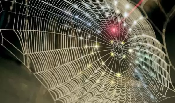
Innovation spins spider web architecture into 3D imaging technology
Innovators are taking cues from nature to develop 3D photodetectors for biomedical imaging.
Purdue University researchers used architectural features from spider webs to develop the technology. Spider webs provide mechanical adaptability and damage-tolerance against various mechanical loads such as storms, the scientists said.
"We employed the unique fractal design of a spider web for the development of deformable and reliable electronics that can seamlessly interface with any 3D curvilinear surface," said Chi Hwan Lee. "For example, we demonstrated a hemispherical, or dome-shaped, photodetector array that can detect both direction and intensity of incident light at the same time, like the vision system of arthropods such as insects and crustaceans."
The U.S. National Science Foundation-funded technology uses the structural architecture of a spider web that exhibits a repeating pattern. The research is published in Advanced Materials.
Lee said this technology provides unique capabilities to distribute externally induced stress throughout the threads according to the ratio of spiral and radial dimensions, and provides greater extensibility to better dissipate force under stretching. Structures can then tolerate minor cuts of the threads while maintaining overall strength and function of the entire web architecture.
"The resulting 3D optoelectronic architectures are particularly attractive for photodetection systems that require a large field of view and wide-angle anti-reflection, which will be useful for many biomedical and military imaging purposes," added Muhammad Ashraful Alam.
Alam said the work establishes a platform technology that can integrate a fractal web design with system-level hemispherical electronics and sensors, offering mechanical adaptability and damage-tolerance against mechanical loads.
"The assembly technique presented in this work enables deploying 2D deformable electronics in 3D architectures, which may foreshadow new opportunities to better advance the field of 3D electronic and optoelectronic devices," Lee said.
Added Khershed Cooper, a program director in NSF's Directorate for Engineering, "These researchers developed a new nanomanufacturing process involving 3D nanoassembly to fabricate plasmonic nanoarchitectures, which can be integrated with diverse substrates for a broad range of applications in imagers, sensors and lasers for the benefit of the U.S. economy and society."


