
Imaging tool may aid nanoelectronics by screening tiny tubes
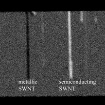
Metallic and semiconducting single-wall carbon nanotubes are distinguished using a new imaging tool for rapidly screening the structures. The technology may hasten the use of nanotubes in creating a new class of computers and electronics that are faster and consume less power than those in use today. (Weldon School of Biomedical Engineering, Purdue University)
WEST LAFAYETTE, Ind. - Researchers have demonstrated a new imaging tool for rapidly screening structures called single-wall carbon nanotubes, possibly hastening their use in creating a new class of computers and electronics that are faster and consume less power than today's.
The semiconducting nanostructures might be used to revolutionize electronics by replacing conventional silicon components and circuits. However, one obstacle in their application is that metallic versions form unavoidably during the manufacturing process, contaminating the semiconducting nanotubes.
Now researchers have discovered that an advanced imaging technology could solve this problem, said Ji-Xin Cheng, an associate professor of biomedical engineering and chemistry at Purdue University.
"The imaging system uses a pulsing laser to deposit energy into the nanotubes, pumping the nanotubes from a ground state to an excited state," he said. "Then, another laser called a probe senses the excited nanotubes and reveals the contrast between metallic and semiconductor tubes."
The technique, called transient absorption, measures the "metallicity" of the tubes. The detection method might be combined with another laser to zap the unwanted metallic nanotubes as they roll off of the manufacturing line, leaving only the semiconducting tubes.
Findings are detailed in a research paper appearing online this week in the journal Physical Review Letters.
Single-wall nanotubes are formed by rolling up a one-atom-thick layer of graphite called graphene, which could eventually rival silicon as a basis for computer chips. Researchers in Cheng's group, working with nanomaterials for biomedical studies, were puzzled when they noticed the metallic nanoparticles and semiconducting nanowires transmitted and absorbed light differently after being exposed to the pulsing laser.
Then researcher Chen Yang, a Purdue assistant professor of physical chemistry, suggested the method might be used to screen the nanotubes for nanoelectronics.
"When you make nanocircuits, you only want the semiconducting ones, so it's very important to have a method to identify the metallic nanotubes," Yang said.
The paper was written by Purdue physics doctoral student Yookyung Jung; biomedical engineering research scientist Mikhail N. Slipchenko; Chang-Hua Liu, an electrical engineering graduate student at the University of Michigan; Alexander E. Ribbe, manager of the Nanotechnology Group in Purdue's Department of Chemistry; Zhaohui Zhong, an assistant professor of electrical engineering and computer science at Michigan; and Yang and Cheng. The Michigan researchers produced the nanotubes.
Semiconductors such as silicon conduct electricity under some conditions but not others, making them ideal for controlling electrical current in devices such as transistors and diodes.
The nanotubes have a diameter of about 1 nanometer, or roughly the length of 10 hydrogen atoms strung together, making them far too small to be seen with a conventional light microscope.
"They can be seen with an atomic force microscope, but this only tells you the morphology and surface features, not the metallic state of the nanotube," Cheng said.
The transient absorption imaging technique represents the only rapid method for telling the difference between the two types of nanotubes. The technique is "label free," meaning it does not require that the nanotubes be marked with dyes, making it potentially practical for manufacturing, he said.
The researchers performed the technique with nanotubes placed on a glass surface. Future work will focus on performing the imaging when nanotubes are on a silicon surface to determine how well it would work in industrial applications.
"We have begun this work on a silicon substrate, and preliminary results are very good," Cheng said.
Future research also may study how electrons travel inside individual nanotubes.
The research is funded by the National Science Foundation.
Writer: Emil Venere, 765-494-4709, venere@purdue.edu
Sources: Ji-Xin Cheng, 765-494-4335, jcheng@purdue.edu
Chen Yang, 765-496-3346, yang@purdue.edu
Related website:
Weldon School of Biomedical Engineering
Note to Journalists: Ji-Xin Cheng is pronounced "Gee-Shin." An electronic copy of the paper is available from Emil Venere, Purdue News Service, at 765-494-4709, venere@purdue.edu
ABSTRACT
Fast Mapping of Metallicity in Individual Single-Walled Carbon Nanotubes Using a Transient Absorption Optical Microscope
Yookyung Jung1, Mikhail N. Slipchenko2, Chang Hua Liu3, Alexander E. Ribbe4, Zhaohui Zhong3, Chen Yang1,4 and Ji-Xin Chen 2,4
1Department of Physics, Purdue University; 2Weldon School of Biomedical Engineering, Purdue University; 3Department of Electrical Engineering and Computer Science, University of Michigan; 4Department of Chemistry, Purdue University
In spite of the outstanding properties of single-walled carbon nanotubes (SWNTs), the co-existence of metallic and semiconducting SWNTs as a result of synthesis has hindered their electronic and photonic applications. We demonstrate a pump-probe microscopy method for fast, contact-free mapping of metallicity in individual SWNTs. We employ the phase of transient absorption as a contrast to discriminate metallic and semiconducting SWNTs. Furthermore, we have clarified the phase dependence on the pump/probe wavelengths and the energy structure of SWNTs. Our imaging method holds the potential of serving as a high-speed metallicity-mapping tool to assist the development of SWNT-based nanoelectronics.