Eric Glover's Lab Notebook
Back to Main Page
Week 01
August 25, 2009 (2 hours):
Met as a team after class to discuss idea for motorized golf cart. It was determined after weighing my set of golf clubs that the cart would need to support a load between 25 and 30 lbs. Cart would use RF signal to follow beacon combined with ultrasonic range finders to detect and avoid objects. The PSSC's would be:
1. Autonomous motorized device capable of moving under its own power
2. Ability to follow a small, wireless transmitter/remote
3. Ability to toggle between "follow" and "rest" modes
4. Ability to sense a number of different hazards (sand traps, water
hazards, trees, golfers, etc.)
5. Ability to keep score for a single golfer
August 27, 2009 (3 hours):
Met as team to discuss preliminary project proposal. Looked at commercially available carts to determine if we could buy something and then modify it for our needs. It was determined that the automated golf cart idea would be too mechanically intensive to make a good project. Decided to switch to a Persistence of Vision (POV) machine. Good examples can be found online. However, we plan to make it unique by incorporating an RF signal to display the image in the direction of the beacon. It will also incorporate an LCD screen and allow the user to input text or images to display on the POV screen. Worked as a team to write and submit preliminary project proposal.
August 28, 2009 (2 hours):
Met as team to discuss block diagram and preliminary PSSC's. Came up with the following list:
1. An ability to display a pattern w/ moving LEDs
2. An ability to track the location of an RF beacon
3. An ability to project pattern in direction of RF
4. An ability to update the pattern and location of display while running
5. An ability to accept user input to change pattern
6. An ability to provide audio feedback to user input
The 6th one may or may not be added - it depends on how much time is left at the end of the semester to add new features. Took notes during meeting and created Block Diagram.
WEEK 01 SUMMARY
Accomplishments: Decided golf cart idea would not work. Decided on new POV machine idea. Submitted preliminary project proposal.
Weekly Work Total: 7 hours
Project Work Total: 7 hours
Week 02
August 31, 2009 (2 hours):
Met as a team to discuss more specific project dimensions and criteria. Decided on a 9"-12" diameter base, 32 RGB LEDs, and an 1800 RPM motor. Discussed having one microcontroller in base unit and one on rotating component. Data would need to be transferred between the two via slip rings or wireless transmission.
September 1, 2009 (2 hours):
Met after class with Russell to work on Powerpoint presentation for class on Wednesday.
September 3, 2009 (1 hour):
Met as team to discuss additional project details and complete Final Project Proposal.
September 4, 2009 (1.5 hours):
Met with Shaun to solder headers onto board and attach wires to necessary pins.
September 6, 2009 (1.5 hours):
Designed preliminary software flowchart and sent out to group for feedback.
WEEK 02 SUMMARY
Accomplishments: PSSC and project proposal finalized. Headers soldered. Preliminary software flow diagram completed.
Weekly Work Total: 8 hours
Project Work Total: 15 hours
Week 03
September 7, 2009 (1 hour):
Met with team to discuss Design Constraint Analysis and assign tasks to each team member. Current tasks are to find suitable LCD screens, shift registers, opto-isolators, batteries, and speakers. Need to complete Component Summary sheet to help determine final parts list.
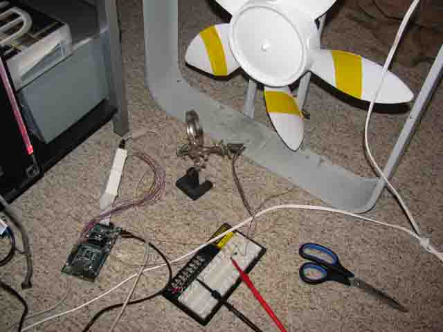
September 8, 2009 (2 hours):
Met with Shaun to test speed of box fan motor. Test setup is shown in following pictures:
Picture 1 Picture 2
Test program determined that box fan speed was between 900 and 1700 RPM. It was thought that the white blades were reflecting ambient infrared light and caused the variance. Yellow duct tape was placed over the blades. The speed reading came in at around 1400RPM but there was still a significant amount of variance. 900 RPM would give an image at 15 frames per second, which would be OK but seem to flicker quite rapidly.
September 10, 2009 (1.5 hours):
Met with team to discuss mounting options for LCD screen and keypad. Discussed use of speaker in final project. Since it is not included as any part of the final PSSC's and it would require a decent amount of hardware and software to implement, it was decided to scrap the speaker idea. Decided to use LCD screen that already exists on the ARM microcontroller instead of purchasing a new one and interfacing it. However, the team will need to come up with some clever mounting or somehow pry the LCD screen from the board and use wires to attach it in order to use it without interfering with the Ethernet port, the headers, and the JTAG connector.
September 11, 2009 (2 hours):
Worked on Team Website. Created separate html pages for Project Description, Contact, Team Members, Notebooks, and Project Documents. These are then displayed using a transparent iFrame. Found background image and wrote the code to display it at 100% of height and width with the text displayed over it.
September 13, 2009 (1 hour):
Researched and found opto-isolator from Fairchild Semiconductor. Wrote Component Summary sheet.
WEEK 03 SUMMARY
Accomplishments: Researched components for Design Constraint Analysis and discussed project features. Tested box fan and determined that it may be too slow for the project.
Weekly Work Total: 7.5 hours
Project Work Total: 22.5 hours
Week 04
September 15, 2009 (2 hours):
Worked with Russell to prepare Design Constraint presentation. Met with Russell and Shaun to discuss methods for transferring data between lower stationary board and upper rotating board. Ideas included 3 microcontroller setup with 2.4GHz wireless connection, slip rings, and optical IR link between the 2 boards. It was decided that slip rings would be too noisy. Identified some potential issues with the optical IR link such as difficulty in construction and decided to go with the 3 microcontroller setup for now.
September 17, 2009 (3.5 hours):
Worked with team to write Design Constraint analysis. Wrote sections on Interface Requirements, On-Chip Peripherals, and Cost Constraints. Document is posted on team website.
WEEK 04 SUMMARY
Accomplishments: Submitted Design Constraint Analysis homework.
Weekly Work Total: 5.5 hours
Project Work Total: 28 hours
Week 05
September 21, 2009 (2 hours):
Met with team to discuss packaging assignment. Came up with a list of parts already ordered or received and also came up with a list of parts that still need to be ordered. The team will need to have most of these parts in hand before making designing the PCB. The team is ordering extras of most of the parts just in case.
Ordered or received
Thermometer (surface mount)
PIC microcontrollers
ARM microcontroller
Phase detectors
Switching 3.3V voltage regulators
Transceiver chips
IR LEDs
IR Sensors
RGB LEDs
AC Motor
Need
BJTs (around 150 of them)
Optoisolators
Relay
Fuses
Fuse blocks
Pushbuttons
Illuminated? Rocker switch
RF SMA connectors
Transmitter packaging
Terminal blocks
MOSFET
Conductive metal cover for RF circuit
Bandpass Filter components
Low dropout 3.3V voltage regulator
Ribbon cable
Connectors
September 24, 2009 (4 hours):
Worked with team to write Packaging Specifications and Design document. Document is posted on team website. Posted additional datasheets on team webpage.
September 25, 2009 (1.5 hours):
Became familiar with PADS program. Finished PADS tutorial on creating footprints. Worked through the end of section 2 of PADS tutorial on power supply design schematic/layout design.
September 27, 2009 (1.5 hours):
Finished remaining parts of PADS tutorial.
WEEK 05 SUMMARY
Accomplishments: Submitted Packaging Specifications and Design document. Became familiar with PADS program.
Weekly Work Total: 9 hours
Project Work Total: 37 hours
Week 06
September 29, 2009 (2.5 hours):
Met with team in Senior Design lab to work on final schematics. Nearly completed schematic for LED Post with LED drivers replacing the shift registers and BJTs that were originally used. Decided to use 2 LED drivers for each color so that each color can be driven by a different current to better match the color intensities. Experimentally determined that blue requires around 4mA to have the same intensity as red and green at 13mA. The LED drivers use the following formula to set output current:
I_out,target = (1.21V / R_ext) * 15.5.
Red, Green: 13mA=(1.21V / R_ext) * 15.5, R_ext = 1440 ohms. The circuit will use R_ext = 1500 ohms.
Blue: 4mA=(1.21V / R_ext) * 15.5, R_ext = 4688 ohms. The circuit will use R_ext = 4700 ohms.
September 30, 2009 (3 hours):
Met with team in Senior Design lab to continue work on final schematics. Finished schematic for LED Post. Worked on schematic for upper board.
October 1, 2009 (10.5 hours):
Met with team in Senior Design lab to finish PADS schematic. Determined the following pin usage for micros 2 & 3:
Micro 2
RB0 - RB7: Data bus connection to Micro 3
RB8 - RB12: Transceiver (DAT, CLK, DR1, CS, CE)
RB13 - RB14: Handshaking for Data Bus communication
Micro 3
RB0 - RB7: Data bus connection to Micro 2
RB8 - RB11: OUT to LED Board
RB12: IR LED Interrupt
Wrote Hardware Narrative report and submitted it.
WEEK 06 SUMMARY
Accomplishments: Finished Schematics.
Weekly Work Total: 16 hours
Project Work Total: 53 hours
Week 07
October 5, 2009 (4 hours):
Read Motorola document on PCB Layout and Design. Met with team to discuss safety issues. It was calculated that the force of rotating the motor at 1800 RPMs would create a force of 543G on the LED post. The components on that PCB could possibly fly off if that force is too much for the solder joints to handle. The LED post could also flex if it is not made of a strong enough material. It was decided to mount the post within two circular acrylic pieces and also to have an acrylic covering for the post to hold the components in and to reinforace the post. The team also conducted a timing analysis. The feedback on HW3 raised a lot of questions about whether the project needs three microcontrollers or just two. The following parameters were considered for the timing analysis:
Each column of LEDs will be on for 176us.
The transceiver can send one byte each 32us.
It takes 12us to shift out all the data required for a column.
Each revolution takes 33.3ms to complete.
The clock speed of the PIC microcontroller is approx. 30ns
After taking into account these parameters, it was determined that one microcontroller will be sufficient. The previous concern was that the microcontroller would miss data on the SPI input from the transceiver when it was busy sending data to the LEDs. However, the clock speed of the PIC is so much faster than the rate that data needs to be sent to the LEDs and the rate that bytes need to be read from the transceiver SPI. One microcontroller should have no issue keeping up with the timing requirements.
October 6, 2009 (6 hours):
Updated upper board schematics to reflect change to one microcontroller. Discussed PIC microcontroller coding strategy. There would be three interrupts that drive operation of this micro. Each 176us an interrupt would be generated for the latching signal to shift data out to the LEDs. This interrupt would have priority 1. The PIC has 8 priority levels for interrupts. After sending out the latching signal, the microcontroller would spend the next 12us shifting data out to be ready for the next column. Each time the SPI has received a byte of information from the transceiver (which could be as often as every 32us) an interrupt would be generated with priority 2. This data would then be read before it was replaced with a new byte of information. Lastly, an interrupt would be generated whenever one full rotation occurred, which would be triggered by the IR LED mounted on the bottom of the spinning disc. This would nominally happen every 33.3ms. This intterupt would be priority 3.
Also completed PCB Layout and Design Narrative presentation for class on Wednesday. It can be found on the team webpage. This presentation focuses on a few specific issues that will need to be considered for the PCB design such as the 1.2GHz RF section and the voltage regulators.
October 7, 2009 (5 hours):
Created list of concerns for PCB Layout and Design.
Signal Routing Concerns
1.2GHz section should be separate from other sections
PWR & GND for 20V 3A section (power passed through slip rings) should be at least 20 mils away from other traces to prevent arcing
Voltage regulators can't have signals crossing underneath - that space is reserved for cooling
Need phase shift of 90 degrees with routing wire leading to second phase detector.
Component Placement
Temperature sensor should be away from power signals to reduce noise
1.2GHz circuit component should be much closer together than wavelength through FRF (~15cm) to avoid picking up signals
Transceivers should have line of sight
Place transceivers close to axis of rotation to limit Doppler Effect frequency shift
LEDs as close together as "solderly" possible for clearer image
LED drivers on back side of LED post, leaving only LEDs on front
RLC loop on 5V switching regulators as close as possible to get tighter regulation
Trace Sizing
3A -> at least 52 mils trace width
2A -> at least 28 mils trace width
1.5A -> at least 24 mils trace width
Transmission line needs to have 50 ohms characteristic impedance for best results
EMI Reduction
Copper pour almost everywhere to reduce noise
Filter capacitor after slip rings to filter out low frequency noise
Shield 1.2GHz transmission line to prevent it from picking up noise
Band pass filter oin 1.2GHz section to keep from picking up extra RF signals in the air
Manufacturing Concerns
Cooling holes (vias) under each surface mount regulator for heat dissipation (according to datasheet)
Vias each square cm in 1.2GHz RF section to tie 2 ground planes together
Laid out circuit components for upper board. Made sure to separate power area and digital logic. Placed bypass capacitors as close as possible to switching logic components.
October 8, 2009 (12 hours):
Met with team to finish PCB Layout and PCB homework. Created net rules and autorouted upper board layout. Added debugging LEDs on three unused ports of the PIC microcontroller in case they are useful later. Put headers around edge of board for easy access to signals. Added small copper segments to fix places that were not routed correctly by the Autoroute feature. Finished lower board layout and routing. Did not put copper pours on any board yet because it would have to be removed to make any changes. This will be done after other eyes have a chance to look at the layout and schematic during the Design Review. Wrote and finished PCB Layout and Design Narrative homework assignment.
WEEK 07 SUMMARY
Accomplishments: Updated schematics. Finished preliminary PCB Layout and PCB homework assignment.
Weekly Work Total: 27 hours
Project Work Total: 80 hours
Week 08
October 14, 2009 (9 hours):
Met with team to prepare for Design Review. Completed slides and practiced presentation. Determined the following items to cover during presentation when discussing PCB Layout:
Transmitter
-J1 is input from battery
-On J3 the two bottom pins should be jumpered together to use battery input. The jumper can be removed to use external power supply (for debugging)
-Batties go into a step-up converter
-There needs to be a lot of space around the power inductor
-All of the RF items need to be close together (oscillator, amplifier, output signal)
-Amplifier needs tons of vias for thermal dissipation and grounding
-Antenna is rubber duck type
Overall EMI Reduction
-Copper pour everywhere to reduce noise
-All of the noise signals will be spread out among the frequency band
Lower Board
-Band pass filter to attenuate signals on other frequencies (cell phones on 900 MHz band are of particular concern)
-Transmission line - 50 ohm characteristic impedance, delay line for 90 degree phase shift
-Relay needs to be far from other component
-Relay input from microcontroller is optically isolated
-Traces in RF section need to be much less than 15 cm (wavelength of 1.2 GHz signal through FRF)
-Vias approximately every square cm to ensure proper grounding
LED Post
-RGB LEDs on one side, everything else on other
-2 Drivers for each color so that intensity for each color can be controlled easily
WEEK 08 SUMMARY
Accomplishments: Finished and presented Design Review presentation
Weekly Work Total: 9 hours
Project Work Total: 89 hours
Week 09
October 20, 2009 (2 hours):
There was a concern brought up during the Design Review that the PIC had no dedicated programming header. Looked into required setup for programming and made needed changes to schematics.
October 21, 2009 (4 hours):
Decided to bring all pins on PIC out to headers. Made changes to schematics for Upper Board. Updated Upper Board PCB layout with new header pins. PADS likes to remove connections to headers when the same pin goes out to more than one header. Manually fixed this problem by adding connections in ECO mode.
October 22, 2009 (6 hours):
Worked on Upper Board PCB layout. Passed FreeDFM test. Noticed that the 5V switching regulator needs the soldermask removed from the area underneath it in order to have proper cooling and grounding. Added labels to silkscreen. Carefully checked each pin to make sure nothing was overlooked on schematic or on PCB connections.
October 23, 2009 (5.5 hours):
Finished Upper Board PCB layout. Printed on 1:1 scale and tested parts. Some pins needed to be lengthened to make soldering easier. Also removed soldermask from area under slip ring connector to allow the tabs on that connector to be soldered to the bottom of the board. Added final top and bottom ground pours. Passed FreeDFM test again. Submitted final PCB.
WEEK 09 SUMMARY
Accomplishments: Finished PCB layouts and submitted final design.
Weekly Work Total: 17.5 hours
Project Work Total: 106.5 hours
Week 10
October 26, 2009 (2 hours):
Met with team to begin work on Software Narrative. Wrote document on PIC Microcontroller Code Organization.
October 29, 2009 (1.5 hour):
Made updated block diagram for PIC Micro. This diagram covers byte handling from the transceiver connection.
NOTE: WAS UNABLE TO DO MUCH ON THE PROJECT THIS WEEK DUE TO SUSPECTED H1N1.
WEEK 10 SUMMARY
Accomplishments: Submitted Software Narrative.
Weekly Work Total: 3.5 hours
Project Work Total: 110 hours
Week 11
November 2, 2009 (2 hours):
Began work on patent liability analysis. Identified two major areas to focus on: Persistence of Vision and RF Angle of Arrival. Located the following patents regarding persistence of vision technology:
Patent 5,748,157: Display apparatus utilizing persistence of vision (12/27/94). This device does not require uniform rotary motion and is hand held.
Patent 5,302,965: Display (10/15/91). This device uses lots of LED columns, requires precise motor speed control, and does not use a microcontroller.
Patent 4,689,604: Moving visual display apparatus (3/3/83). This device operates at 1200-1800RPM, uses a microprocessor, and uses 3 LED bars.
The POV Machine that Team 7 is building operates at 1800 RPM but does not require precise motor speed control. It uses stationary and rotary components. It uses a single bard of RGB LEDs instead of multiple bars like several of the devices that are patented. Data is transferred using a wireless transceiver.
November 3, 2009 (2 hours):
Made Patent Liability Presentation for the TCSP section on Wednesday. The presentation can be viewed on the Team 7 homepage under the Design Documents tab.
November 5, 2009 (8 hours):
PCBs arrived. Successfully completed practice surface mount soldering chip. Soldered power supply components on upper board. Tested 5V regulator output and saw +4.996 volts on the DMM. Also started on soldering the LED post.
After beginning soldering of the Upper Board, it was noticed that not all of the connections are correct. It appears that there were a few mistakes made when the PCB was designed. Fortunately there are no deal-breakers. The problems are listed below:
-Pins PGD2 and AN11 are connected together
-!MCLR on J7 and J9 are not connected micro pin 1; instead pin 1 is connected to OUT1 on header J5
-Component U8 is not needed
-Component R10 is not needed
-Component C14 is not needed
-PGD2 on J7 and J10 are not connected to micro pin
-Power Good from 3.3v regulator connected to 1A on header J5 instead of pin 1
-IN1 connected to 1B and not pin 1
Solution: Connect 1A, 1B, and OUT1 together. Also, program using AN11, PGC2, and OUT1. It appears that what happened was the schematics were updated but the changes were not transferred to the PCB layout even though they were linked in PADS at the time and a new net list was sent.
Started and completed Patent Liability Analysis paper.
November 6, 2009 (3 hours):
Met with team to continue work on soldering. Tested 3.3 volt output on upper board power supply and saw that it was giving the correct voltage. Tested connections on LED Post and it appears that the PCB was made correctly.
WEEK 11 SUMMARY
Accomplishments: Completed Patent Liability Analysis. Started work on soldering PCBs.
Weekly Work Total: 15 hours
Project Work Total: 125 hours
Week 12
November 9, 2009 (1.5 hours):
Continued work on soldering. Added remaining components for LED post. Russell built a test circuit but only the first 16 LEDs turned on and these LEDs showed yellow. The test circuit is designed to put a 1 on all of the outputs of the LED drivers. Something must be wrong between drivers 2 and 3.
November 10, 2009 (3 hours):
Team met to work on LED Post and to test the output on the voltage regulators. Resoldered LED drivers and now the LED Post works! Video is posted on YouTube. Hooked up regulator outputs to oscilloscope. There is a lot of switching noise and some work needs to be done to produce a cleaner output. It is unknown at this point whether the output will affect the performance of the project.
November 12, 2009 (1.5 hours):
Began working with MPLab to learn how to write code for the PIC24F.
November 13, 2009 (2 hours):
Continued work with MPLab. Read through reference documents on SPI and Interrupts on the PIC24F. Created connector for the upper board to add in a snubber circuit. This may fix the switching power supply problems.
WEEK 12 SUMMARY
Accomplishments: LED Post works completely! Team submitted Reliability and Safety Report.
Weekly Work Total: 7 hours
Project Work Total: 132 hours
Week 13
November 16, 2009 (1.5 hours):
Wrote a small test program to simply blink a light on the Explorer 16 Development Board. Sample code can be found here. Works without any issues. It was suggested to the team that we test the power supply on a different oscilloscope. The ripple is much better on the different oscilloscope. The probe must be bad on the first scope. The project can proceed now that the power supply is operating at an acceptable output.
November 18, 2009 (5 hours):
Soldered remaining components on upper board PCB. Had to create a connector to solder 1A, 1B, and OUT1 so that there is a wired OR connection leading into the !MCLR signal on the microcontroller. Also soldered flywire from this connection to the !MCLR header since when the PCB was made this connection was missing. Also had to flywire between the PGD2 pin on the microcontroller and its header. This connection was also not made when the PCB was designed. Wrote a test program to turn on the 3 debugging LEDs (AN10, AN11, and AN12). It works!!! This means that the Upper Board PCB is working as designed.
November 19, 2009 (10 hours):
Worked on writing additional test programs for the PIC. Wrote program to generate interrupt when the IR LED signal is high. The code can be found here. After this was proven to work, wrote program to send data to the LED post. This was done using a manual clock and data line instead of using SPI for this initial test code. It was determined that pins TD0 and TCK do not work. Wrote test program to turn all PORTB pins high. Again, these pins did not respond. It was thought that perhaps these pins were fried. Removed PIC and put on a new one. The same problem was found. Looked through documentation and finally figured out that those pins are multiplexed with the JTAG connector. The JTAG connector needs to be disabled using the line:
_CONFIG1 ( JTAGEN_OFF )
This allowed those pins to work. Wrote a program to slowly clock in data to the LED post and it works!
November 20, 2009 (3 hours):
Worked on sending data to the LED Post using the SPI Module. This worked without too much trouble. Wrote some fun test programs to display different patterns. Displayed these patterns by waving the LED Post around. This example code displays a checkerboard with alternating blue and blank colors.
WEEK 13 SUMMARY
Accomplishments: Upper board is completely functional.
Weekly Work Total: 19.5 hours
Project Work Total: 151.5 hours
Week 14
November 23, 2009 (6 hours):
Determined that external oscillator is not working. Read through a myriad of datasheets on coding with the external oscillator. Tried setting the configuration bits to start up with external oscillator and also tried switching to external oscillator after starting up with FRC. Tried everything. No luck :-(. Also wrote test program making use of an external interrupt (for the IR sensor). At least that worked!
November 24, 2009 (2 hours):
Soldered on new oscillator of different type. Again no luck getting the external oscillator to work. Wrote code to test the ability to make TMR interrupts. The test was successful.
WEEK 14 SUMMARY
Accomplishments: Determined several ways how to not get the external oscillator to work. Wrote test code and determined individual functionality of TMR interrupts and external interrupts.
Weekly Work Total: 8 hours
Project Work Total: 159.5 hours
Week 15
November 30, 2009 (8 hours):
Now that each individual module for the microcontroller code appears to be working, the whole upper PIC code could be put together. There were surprisingly few problems getting the different segments together into one code document. It was set up so that a trigger by the IR sensor would start the process of shifting data out to the LED post. After this, created the first ever pixel map for The Flying Bits! It was first drawn in Microsoft Paint. The intended image looks like this:

After drawing the image in Paint, it was manually converted to a series of hex codes - with 2 bytes used per column. The most significant bit of the first byte is at the top of the image. The most significant bit of the second byte is halfway down the image (pixel 17, where the top pixel is pixel 1). The initialization of the array to show the happy face is located here. Wrote a function to handle an input array and shift it out in the correct fashion. It is located here. The image can be seen by waving the LED post, but unfortunately the packaging is not complete yet so it can not be seen like it is supposed to.
December 1, 2009 (4 hours):
Started working on initialization of the transceiver module. It appeared that some of the port pins were not working. Some pins could not be declared as digital inputs!! Tried setting all pins as inputs and then tying them high by placing a connection between the pin and +3.3V through a 10K resistor. Some pins worked, and some pins didn't. Noticed that the pins that didn't work were ones that were called AN0-AN11. Hmm.... Scavenged through documentation and found that the following line of code needs to be inserted to be able to use these pins as digital inputs instead of analog inputs:
AD1PCFG = 0x1FFF; //set up as digital i/o pins
Beware future PIC24F users! Also found out that OSCIOFNC_ON needs to be in the _CONFIG2 section in order to use the SOSC pins as digital I/O. To recap, now the items under _CONFIG1 and _CONFIG2 are as follows:
_CONFIG1 ( JTAGEN_OFF & GCP_OFF & GWRP_OFF & COE_OFF & FWDTEN_OFF & ICS_PGx2)
_CONFIG2 ( POSCMOD_NONE & FCKSM_CSDCMD & FNOSC_FRCPLL & OSCIOFNC_ON)
The team should no longer have any problems with initializations and be able to use port pins to their full effectiveness. That was the big victory of the night.
December 2, 2009 (10 hours):
Russell decided to create a Canadian pixel map instead of sleeping. It was made in Excel. Created separate pages for the three different colors (Red, Green, Blue) and then calculated hex codes. These were then exported to a .csv file so that the output can quickly be loaded into an array in the program. RED, GREEN,BLUE. Took on the challenge of making an American flag using the same process. This file contains a different pixel map, but it shows the process of creating a new one. First an image is drawn using R for Red, B for Blue, G for Green, W for White, etc... Then a different sheet is made for Red, Green, and Blue. For each sheet, if that color is contained in that spot, a 1 is placed. Otherwise, a 0 is. Then a formula is used to calculate the hex codes. This is sent to a .csv and then loaded into an array in the program! It is somewhat time consuming, but it works! Shaun promises he will have a LabVIEW program soon that does it for us. Steve and Shaun got the motor mounted and started spinning up the project! Loaded pixel maps onto the upper PIC and started seeing some great results. A video is posted on YouTube and on the Team 7 main page. Things are progressing nicely.
December 3, 2009 (12 hours):
Worked with Russell to start testing the uMIRF transceiver. Since the ARM was at Shaun's apartment and it might have trouble with the low-level operations that the transceiver requires, it was decided to solder up another PIC board to act as the transmitter while the upper PIC would be the receiver. Checked on the scope and found that the transceivers were being initialized correctly. However, the link is not working as expected. The transmitter is constantly transmitting data and is using SPI. The upper PIC is using SPI out to initialize the transceiver and then remapping these pins to SPI in to receive data. Perhaps this is not working correctly? Found some sample code online. The sample code is very similar to ours except that all of the data sending is clocked manually instead of using SPI.
December 4, 2009 (4 hours):
Continued working on debugging the transceiver. It appears that the transceiver is trying to drive the SPI in pin to the correct values, but the upper PIC is acting like that pin is still an output. The data being sent is "0xAAAA" and it can be seen on the scope, but the pin is only driving from 0 to 0.1 V instead of from 0 to 3.3V. The next test should be to initialize the transceiver manually instead of using SPI.
WEEK 15 SUMMARY
Accomplishments: Figured out the correct initializations for the PIC24F. Compiled separate working code snippets into one main program. Determined pixel map array format and successfully generated first pixel map! (smiley face)
Weekly Work Total: 38 hours
Project Work Total: 197.5 hours
Week 16
December 6, 2009 (10 hours):
Russell wrote a function to manually clock out data to the transceiver. It still didn't work. Shortened the delays between the transceiver writes and reads and now it works! This appears to be a very time critical process. The data was shifted out to the LED post so that it is clear what data is being received on the transceiver link. For some strange reason, the final bit is randomly driven high! Then the line simply decays instead of being driven low. Checked to see if the problem could be fixed by sending more than one byte at a time. It doesn't help. Decided to simply send more bits than necessary and ignore the last few. The packet is set up as follows (by bit):
15: blank image
14: new image?
13-10: image # to display (0-15)
9-4: angle offset (0-35, then multiplied by 10).
3-0: Don't care
December 7, 2009 (10 hours):
Continued work on code. Incorporated new transceiver code into main code and wrote function to interpret data sent over the transceiver link. Created new pixel map that said "Team 7". It looked like a kindergartener drew it, so the direction on the "e" was switched to make it look even more like it.

Steve drew a block P pixel map that looks really awesome. He used Shaun's new LabVIEW "paint" program. Unfortunately the output array is a little off. The image showed up upside down and the wrong side was on top! Quickly made Excel workbook to fix it. The image looks great.

December 8, 2009 (12 hours):
First all-nighter of the semester. Started out by going through the upper PIC code with Russell to determine areas where timing could be improved. It was noticed that the image would flicker occassionally and it appears to be a software issue. The order was changed so that the data is sent to the LED drivers immediately after the previous data was latched. This way the only item in the TMR interrupt is the latch. The ISRs should be as short as possible to prevent possible timing issues. The output is much better now. Spent most of the night trying to get the 1.2 GHz RF transmitter to work. The scope proved that the correct initialization data was being sent. However there were problems with the clock signal. A port pin on the microcontroller was used generate the clock signal at 200 kHz. However the output was only driven from around 0 to 1.2V. It was found that there were some wires accidentally soldered together and it was creating a heavy load on the clock signal. Russell fixed this and the clock signal worked properly. However the PLL failed to achieve a digital lock and the transmitter is not working. It is suspected that not enough power is coming back to the feedback input of the PLL. This is a hard circuit to debug and it is ultimately unrelated to the project. It would just be a cool feature to be able to have the image follow the user around. A new pixel map was created that shows "IU" and then a few seconds later shows "SUCKS". This was the team's first time using a non-static pixel map. It would not be too hard to move on to showing animations! This should be the final PSSC and it should replace the RF beacon one. Shaun updated the menu on the ARM. The ARM and the lower PIC communicate using 6 data lines and the relevant information is then sent through the wireless transceiver to the upper PIC. The ARM sends a number between 0 and 63 to the lower PIC based on the user menu selection and the PIC reads this value every 500 ms or so.
0: blank display
1-15: preset image
16: custom image (not used currently)
17-54: angle offset (0 to 35)
55-63: unused
December 9, 2009 (1 hour):
Presented to class. Asked Dr. Meyer about changing the RF beacon PSSC to one about displaying animations. Meyer was willing to accept the change.
Slept a long time after pulling the all-nighter!
December 10, 2009 (16 hours):
Steve painted box at his apartment. While he was doing that, the rest of the team worked on creating new pixel maps. Created hilarious one of dinosaur walking. In the code, the angle offset is also incremented so that it appears that the dinosaur is walking in circles around the machine.

Went over to Steve's apartment to pick up the box. Came back and re-mounted everything inside and above the box. Had to cut down the number of pixel maps in the code to get it to compile. It uses 99% of the available memory! See it in a picture here. The project was complete at around midnight. The team went over to EE 129 and watched it in the dark. And then.......
DISASTER STRIKES!
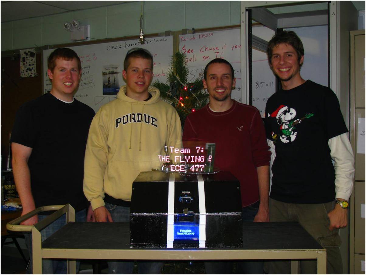
We smelled burning so the machine was turned off and the team opened up the project. The motor was incredibly hot. We let it cool down for a while and tried turning it back on. Nothing happened. The motor overheated and most likely blew the 4 uF capacitor. Looking back, the team is lucky that a fire wasn't started, which could have destroyed the entire project. The motor was replaced with a new one. What was going to be an early night turned into an all-nighter as the packaging was basically rebuilt. It is believed that the cooling fan did not turn on. The cooling fan is very finnicky - it will only turn on after a power cycle when it has come to a complete stop and the user waits for 5 seconds or more before applying power. There was also no air inlet - only an air outlet. A new hole was drilled. The project was finally working at around 6 in the morning. It worked as before although it appears that the IR LED does not trip every time and the picture flickers a bit more. The team messed with it for a bit before giving up and deciding it was good enough. Then a video was created for the presentation to EE 362 that went over the user menu. Also a team picture was taken.
WEEK 16 SUMMARY
Accomplishments: Finished project! Packaging complete. Code complete. Generated a myriad of pixel maps. Presented to ECE 362. Salvaged success out of a near-disaster.
Weekly Work Total: 49 hours
Project Work Total: 246.5 hours
Week 17
December 13, 2009 (1.5 hours):
Wrote individual contributions page and sent to Steve to include in Final Report.
December 14, 2009 (2 hours):
Went through both PIC c files and added function headers detailing each function along with inputs, returns, dependencies, a description, and revision history.
WEEK 17 SUMMARY
Accomplishments: Wrote individual contributions page. Updated function headers in the software to prepare for final submission. Submitted final reports.
Weekly Work Total: 3.5 hours
Project Work Total: 250 hours